
Réponse directe
Evaluate SMT assembly risk from FOPLP and thermal processing trends by reviewing package warpage data, reflow profile parameters, board stackup, and MSL handling before committing to a build. Fan-out panel-level packaging introduces larger, thinner bodies with unique coplanarity behavior, while lead-free thermal budgets demand tighter control over ramp rate, soak, and peak temperature. These variables directly affect solder joint integrity, inspection strategy, and overall yield.
Why FOPLP Changes the Risk Equation in SMT Assembly
Fan-out panel-level packaging shifts the risk profile for SMT assembly because the package form factor behaves differently from a conventional BGA. FOPLP packages are manufactured on large panels rather than round wafers, which allows more chips per panel and lower cost per unit. But that manufacturing efficiency comes with a mechanical trade-off: the package body is often larger, thinner, and more susceptible to warpage during reflow.
The warpage behavior of a FOPLP package depends on the panel construction, mold compound properties, redistribution layer (RDL) design, and the silicon-to-mold ratio. A package that looks flat at room temperature can bow significantly at reflow temperatures, especially if the coefficient of thermal expansion (CTE) mismatch between the silicon die, mold compound, and copper RDL is not well balanced. This warpage directly impacts solder joint formation because the package's bump coplanarity changes as the assembly heats up.
For the PCB designer, the practical implication is that you cannot treat a FOPLP package like a standard BGA of similar pin count. The larger body size means more distance between the package center and the corner bumps, which amplifies any warpage. A 30 mm x 30 mm FOPLP package will show more edge lift at peak temperature than a 15 mm x 15 mm package with the same material set. That edge lift can cause corner solder joints to open or form head-in-pillow defects.
Another factor is the panel-level manufacturing process itself. Because FOPLP packages are processed on panels, the mold compound and RDL layers can have thickness variations across the panel. This means two packages from the same panel may have slightly different warpage characteristics. Your EMS partner should treat FOPLP components as a statistical distribution rather than assuming identical behavior from every unit.
The thermal processing trend compounds this risk. Lead-free solder alloys require higher peak reflow temperatures, typically in the 240°C to 260°C range, compared to older tin-lead profiles. Higher temperatures increase the thermal gradient across the package and the PCB, which can worsen warpage. Faster ramp rates, often used to reduce cycle time, can also create larger temperature differentials between the package surface and the board, increasing the risk of solder joint defects.
Thermal Processing Variables That Matter More Than Peak Temperature
Engineers often focus on peak reflow temperature as the primary thermal risk factor, but the full profile matters more. Ramp rate, soak time, time above liquidus, and the cooling rate all influence how a FOPLP package behaves during assembly.
The ramp rate controls how quickly the package and board heat up. A fast ramp rate, such as 2°C to 3°C per second, can create a significant temperature delta between the top surface of the package and the PCB underneath. This delta causes differential expansion, which can increase warpage and stress on the solder joints. Slower ramp rates, around 1°C per second, give the package more time to equilibrate with the board temperature, reducing the thermal gradient.
Soak time is the period where the assembly is held at a moderate temperature, typically 150°C to 190°C, to allow the flux to activate and the board to reach a uniform temperature. A longer soak can help equalize temperatures across the assembly, but it also exposes the package to elevated temperatures for a longer duration. For FOPLP packages with moisture sensitivity, a longer soak may increase the risk of moisture-induced delamination or popcorning.
Time above liquidus (TAL) is the duration the solder remains molten, usually 60 to 120 seconds for lead-free profiles. Longer TAL allows better wetting and self-alignment, but it also keeps the package at high temperature for longer, which can increase warpage and intermetallic compound growth. For FOPLP packages with fine-pitch bumps, a shorter TAL may be necessary to limit the time the package is in its most warped state.
The cooling rate also matters. A fast cooling rate can freeze the solder joint in a stressed state if the package and board contract at different rates. A slower cooling rate gives the assembly more time to relax, but it also extends the total thermal exposure. The optimal cooling rate depends on the specific package and board combination.
The CTE Delta Between Component and Board
The coefficient of thermal expansion (CTE) mismatch between the FOPLP package and the PCB is a critical variable. A typical FR-4 board has a CTE of 14 to 17 ppm/°C in the X-Y plane, while a silicon die has a CTE of about 3 ppm/°C. The mold compound and RDL materials in a FOPLP package are engineered to bridge this gap, but the effective CTE of the package depends on the ratio of silicon to mold compound.
For a large FOPLP package, the CTE mismatch with the board can cause significant shear stress on the solder joints during cooling. This stress is highest at the corners of the package, where the distance from the neutral point (DNP) is greatest. If the board is thin or has uneven copper distribution, the board can also warp, adding to the stress on the solder joints.
When evaluating risk, you need to compare the package's effective CTE to your board's CTE. A board with heavy copper planes, such as 2 oz or 3 oz copper, will have a lower effective CTE than a board with light copper distribution. A thicker board, such as 2.4 mm, will resist warpage better than a thin 1.0 mm board, but it will also create a larger thermal gradient during reflow.
Reflow Profile Verification with Thermocouples
Before committing to a full production run, you should verify the thermal profile on a test board. Place thermocouples on the FOPLP package body, on the PCB surface near the package, and on the bottom side of the board. Run the board through the reflow oven with the proposed profile and record the temperature data.
The key data points to compare are the peak temperature at the package body versus the PCB surface, the time to reach peak temperature, and the cooling rate. A large delta between the package and board temperatures indicates a high thermal gradient, which increases warpage risk. If the delta is more than 10°C to 15°C, you may need to adjust the profile or reconsider the board stackup.
For quantitative warpage data, shadow moiré or digital image correlation (DIC) can measure the package's warpage at reflow temperatures. These methods require specialized equipment, but they provide the most accurate picture of how the package will behave during assembly. If you do not have access to these tools, request warpage data from the component supplier, ideally measured at J-STD-020 reflow conditions.
> Practical note: A thermocouple attached to the package body with high-temperature tape will read closer to the true package temperature than one attached to a nearby solder joint. Always place at least one thermocouple directly on the package surface for FOPLP components.
Moisture Sensitivity, Floor Life, and Bake Requirements
FOPLP packages, like other plastic-encapsulated components, have a moisture sensitivity level (MSL) rating defined by J-STD-020. The MSL rating determines how long the component can be exposed to ambient humidity before reflow without requiring a bake. FOPLP packages with large bodies and thin mold compound are often rated MSL 3 or MSL 4, which means they have a floor life of 168 hours or 72 hours, respectively, at 30°C/60% RH.
The risk comes from moisture absorbed by the mold compound. During reflow, the moisture vaporizes rapidly, creating internal pressure that can cause delamination, cracking, or popcorning. For a large FOPLP package, the risk is higher because the moisture has a longer path to escape and the package has more surface area for moisture ingress.
When evaluating assembly risk, you need to check the MSL rating of every FOPLP component in your BOM and compare it to your actual assembly schedule. If the components have been sitting in inventory for more than their floor life, they will need to be baked before assembly. The bake time and temperature are specified in J-STD-033 and typically range from 24 to 192 hours at 125°C, depending on the MSL level and package thickness.
The bake requirement interacts with your thermal processing plan. Baking at 125°C for an extended period can affect the solder balls or bumps on the package, and the bake must be completed before the components are exposed to the reflow profile. If your EMS partner receives the components and must bake them, that adds lead time to the assembly schedule. You should include this in your project timeline and communicate it in the RFQ.
Another common mistake is assuming that all packages with the same MSL rating behave the same. The MSL rating is a maximum allowable exposure time, but the actual moisture absorption depends on the package construction. A FOPLP package with a thin mold cap will absorb moisture faster than a thicker package. If you have a long assembly schedule, consider using a moisture barrier bag with desiccant and a humidity indicator card to track exposure.
Stencil Design and Solder Paste Printing with Mixed Component Types
When you mix FOPLP packages with conventional BGAs and SMT components on the same board, the stencil design becomes a critical risk factor. FOPLP packages often have fine-pitch bumps or pads that require a thinner stencil or smaller aperture to achieve the correct paste volume. A conventional BGA may need a thicker stencil to deposit enough solder for its larger ball pitch.
The challenge is that a single stencil must accommodate both requirements. A step stencil, where the thickness is reduced in specific areas, can be used to provide a thinner aperture for the FOPLP package while maintaining a thicker section for other components. However, step stencils are more expensive and require careful design to ensure the step transition does not cause paste smearing or insufficient deposition.
The larger body size of a FOPLP package can also shadow adjacent components during printing. The squeegee may not be able to deposit paste evenly in the area immediately around the package, especially if the package is tall or the adjacent components are low-profile. You may need to adjust the print direction or use a different squeegee angle to ensure complete paste deposition.
Paste release is another critical variable. FOPLP packages with fine-pitch pads require good paste release from the stencil aperture to achieve the correct paste volume. Aperture wall finish, stencil material, and the type of solder paste all affect release. A laser-cut stencil with electropolished apertures and a nano-coating can improve release for fine-pitch applications.
Practical Example: Mixed BGA and FOPLP Board
Consider a board with a 25 mm x 25 mm FOPLP package, a 15 mm x 15 mm BGA, and several 0402 passive components. The FOPLP package has 0.4 mm pitch bumps, while the BGA has 0.8 mm pitch balls. The recommended stencil thickness for the FOPLP package is 0.100 mm, while the BGA would typically use a 0.125 mm stencil.
A step stencil with a 0.100 mm thickness in the FOPLP area and 0.125 mm elsewhere can work, but the step transition must be placed at least 3 mm away from the FOPLP pads to avoid paste smearing. The aperture area ratio for the FOPLP pads must be above 0.66 for good paste release, which means the aperture width must be at least 0.066 mm for a 0.100 mm stencil. If the pad size is smaller, you may need a thinner stencil or a different paste.
The print direction should be set so that the squeegee does not drag paste away from the FOPLP area. If the FOPLP package is near the edge of the board, you may need to adjust the board orientation in the printer. A first-article inspection after printing should include paste height measurement on the FOPLP pads to verify the deposited volume.
Inspection Methods for FOPLP Solder Joints
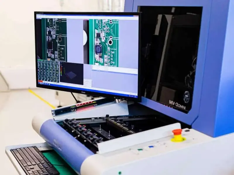
After reflow, FOPLP solder joints are hidden under the package, so visual inspection and automated optical inspection (AOI) cannot verify the joint quality. X-ray inspection is essential for FOPLP assemblies. A 2D X-ray system can detect gross alignment issues, solder voids, and bridging, but it cannot easily distinguish between a well-formed joint and a head-in-pillow defect where the solder ball and paste do not fully coalesce.
For critical applications, 3D X-ray (computed tomography, or CT) provides a cross-sectional view of the solder joints and can reveal internal voiding, joint shape, and the presence of head-in-pillow defects. CT inspection is slower and more expensive than 2D X-ray, so it is typically used for first-article inspection or for a sample of production units rather than 100% inspection.
AOI can still be used to check for missing components, gross misalignment, and correct polarity before X-ray inspection. The AOI system can also verify that the FOPLP package is seated correctly and that there are no visible solder balls or debris on the board surface.
When setting up the inspection plan, consider the defect modes most likely for FOPLP assemblies. Warpage-induced opens are most likely at the corners of the package, so the X-ray inspection should prioritize those areas. Head-in-pillow defects are more likely with fine-pitch bumps and fast ramp rates, so the X-ray operator should know what to look for.
> Practical note: For a mixed assembly with FOPLP and conventional BGAs, use 2D X-ray for 100% inspection of all BGA and FOPLP joints, and reserve CT for the first article and for any units that show anomalies on the 2D X-ray.
Erreurs courantes et quand impliquer votre partenaire EMS
Engineers make several common mistakes when evaluating FOPLP and thermal processing risk. The most frequent is focusing only on peak reflow temperature and ignoring ramp rate, soak time, and cooling rate. Another is assuming that all packages of the same size behave the same, when in fact FOPLP warpage depends heavily on the internal construction.
A third mistake is not checking the MSL and floor life of FOPLP components against the actual assembly schedule. If components have exceeded their floor life, they must be baked, which adds time and can affect the solder balls. A fourth mistake is designing the stencil without considering the mixed component types, leading to insufficient paste on the FOPLP pads or excessive paste on the BGA.
You should involve your EMS partner early in the design review process. Share the FOPLP package datasheets, warpage data, and MSL ratings. Provide the PCB stackup, copper weight, and board thickness. Discuss the proposed reflow profile and any thermal constraints from adjacent components, such as electrolytic capacitors or connectors that cannot withstand high temperatures.
The RFQ should include all of this information so the EMS can evaluate the risk before quoting. Include the complete BOM with package dimensions, MSL level, and any supplier warpage specifications. State your expected reflow profile and whether you have a preferred solder paste. Also share any known thermal constraints from adjacent components.
Early communication can prevent surprises. If the EMS identifies a warpage risk, you may need to adjust the board stackup, add a stiffener, or change the reflow profile. These changes are much easier to make before the board is fabricated and the components are sourced. For related risk factors, review how inventory and sourcing trends affect component availability and lead times, and how leadership and sales trends influence supplier priorities. Additionally, consider the impact of PCB assembly and COB trends on your assembly strategy, and stay informed about the broader PCB market and industry outlook. Finally, evaluate PCB fabrication and sourcing trends that can affect board quality and delivery.
Omini, as an EMS partner, can help you evaluate these risks during the design for manufacturability (DFM) review. By providing detailed package and board data early, you enable a more accurate risk assessment and a smoother path to production. The goal is to identify and mitigate thermal and warpage risks before they become yield problems on the line.
> Engineering handoff note: How to Evaluate SMT Assembly Risk from Inventory and Sourcing Trends, How to Evaluate SMT Assembly Risk from Leadership and Sales Trends, and How to Evaluate SMT Assembly Risk from PCB Assembly and COB Trends before the release package is frozen.
> Also compare How to Evaluate SMT Assembly Risk from PCB Market and Industry Outlook Trends and How to Evaluate SMT Assembly Risk from PCB Fabrication and Sourcing Trends before locking the quote scope.
> Engineering handoff note: How to Evaluate SMT Assembly Risk from Sourcing and Expansion Trends before the release package is frozen.
> Engineering handoff note: How to Evaluate SMT Assembly Risk from Manufacturing Capacity and Stencil Trends before the release package is frozen.
> Engineering handoff note: How to Evaluate SMT Assembly Risk from Sales and Electronics Trends before the release package is frozen.