
Direkte Antwort
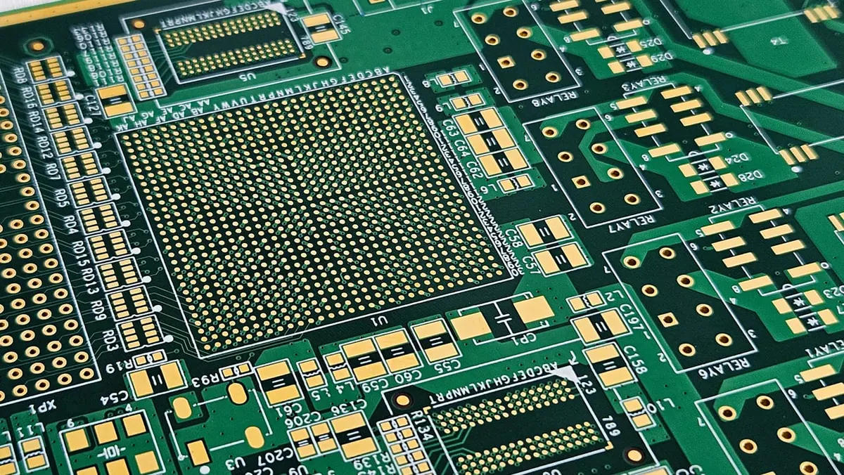
HDI printed circuit boards use laser-drilled microvias, finer trace widths, and sequential lamination to achieve higher wiring density in a smaller footprint. This makes them essential for compact, high-performance electronics where standard through-hole vias and wider traces cannot meet routing demands. The key characteristics—microvia structures, layer build-ups, material constraints, and via-in-pad processing—directly affect your design rules, fabrication cost, assembly yield, and long-term reliability.
What Defines an HDI PCB: Microvia Technology and Layer Build-Ups
An HDI board is not simply a standard PCB with smaller vias. The defining feature is the microvia, a laser-drilled hole typically 0.075 mm to 0.15 mm in diameter that connects adjacent or nearby layers. Unlike mechanical through-hole vias that penetrate the entire board, microvias are blind (connecting an outer layer to one or more inner layers) or buried (connecting inner layers only). This allows routing to escape from fine-pitch BGA packages without consuming every available channel on outer layers.
The second defining characteristic is sequential lamination. A standard multilayer board is pressed once with all copper layers and prepreg stacked together. An HDI board is built in stages: an inner core is laminated, drilled, plated, and then additional layers are laminated on top. Each lamination cycle adds cost and lead time, so the number of build-up cycles directly correlates with board price.
HDI Types and Layer Build-Up Structures
The industry classifies HDI boards by their build-up structure:
| HDI Type | Structure | Typical Use Case |
|---|---|---|
| 1-N-1 | One sequential lamination on each side of a standard core | Moderate density, 6–8 layer boards |
| 2-N-2 | Two sequential laminations per side | High-density BGA routing, 10–14 layers |
| 3-N-3 or higher | Three or more build-up cycles per side | Ultra-dense designs, 16+ layers |
| Any-layer HDI | Every layer can connect via stacked microvias | Maximum routing flexibility, highest cost |
The "N" in this notation represents the number of standard core layers. A 1-N-1 board has one microvia layer on each side of the core; a 2-N-2 has two. Each additional build-up step requires its own lamination, drilling, plating, and imaging cycle, which is why cost escalates quickly with HDI type.
Stacked vs. Staggered Microvias
Within a build-up layer, microvias can be arranged in two ways. Staggered microvias are offset from each other and connect only adjacent layers. Stacked microvias sit directly on top of one another, allowing a signal to pass through multiple layers vertically. Stacked vias require filled and plated structures to maintain reliability, especially when they terminate on a BGA pad. Staggered vias are simpler to fabricate and less expensive, but they consume more routing area because each via needs its own landing pad.
For most designs, staggered vias are sufficient. Use stacked vias only when you need to route directly under a BGA pad or when signal integrity demands a short vertical path. If you are unsure which structure your design requires, review the fan-out pattern of your highest-density component before committing to a stackup.
Material Selection and Copper Weight for HDI Fabrication
Material choice in HDI is more constrained than in standard PCB fabrication because thin dielectrics and laser drilling impose specific requirements. Standard FR-4 can work for simple 1-N-1 designs, but higher layer counts and finer features benefit from materials with stable dielectric constant and low dissipation factor.
Thin Cores and Prepreg Systems
HDI build-ups use thin cores, typically 0.05 mm to 0.10 mm, to keep the overall board thickness manageable. These thin cores require resin systems that flow consistently during lamination and maintain uniform thickness across the panel. If the dielectric thickness varies, impedance control becomes difficult, especially for differential pairs running at 100 ohms or single-ended traces at 50 ohms.
For high-speed signals, consider low-loss laminates such as Megtron 6, Rogers 4000 series, or Isola FR408HR. These materials maintain stable electrical properties across frequency and temperature. However, they cost more and may have different drilling parameters than standard FR-4. For a practical comparison of material properties, review the options in Comparing Different Types of Printed Circuit Board Materials before finalizing your stackup.
Copper Weight and Trace Geometry
Standard HDI boards use 0.5 oz (18 µm) or 1 oz (35 µm) copper on outer layers. Inner layers often use 0.5 oz copper to achieve finer line widths. The minimum trace width and spacing depend on the copper weight: 0.5 oz copper supports 75 µm lines with 75 µm spacing in production, while 1 oz copper typically requires 100 µm lines or wider.
Heavier copper increases the minimum feature size because etching becomes less precise with thicker metal. If your design needs 50 µm lines, you must use 0.5 oz or lighter copper. This affects current-carrying capacity, so verify that your trace widths can handle the required current before reducing copper weight for density reasons.
Impedance Control Considerations
Impedance in HDI boards depends on trace width, dielectric thickness, and copper weight. The thin dielectrics used in HDI build-ups naturally bring reference planes closer to signal traces, which reduces the trace width needed for a given impedance. A 50-ohm trace on a 0.1 mm dielectric may be only 0.15 mm wide, whereas the same impedance on a 0.2 mm dielectric requires a wider trace.
This is advantageous for density but creates a manufacturing constraint: the fabricator must control dielectric thickness tightly across the panel. If you require impedance tolerance of ±10% or tighter, specify this on your fabrication drawing and request impedance coupons on the production panel. The Circuit Board Manufacturing Process: A practical reference for Beginners explains how these coupons are used during fabrication and testing.
Microvia Design Rules: Aspect Ratios, Capture Pads, and Via-in-Pad
Microvia design rules differ from through-hole via rules in several important ways. Understanding these constraints early prevents costly design revisions and fabrication delays.
Aspect Ratio Limits
The aspect ratio of a microvia is the ratio of its depth to its diameter. For laser-drilled microvias, most fabricators limit this to 1:1 or slightly higher, meaning a 0.1 mm diameter via can drill through a dielectric thickness of approximately 0.1 mm. If you need to connect through a thicker dielectric, you must either increase the via diameter or use a stacked structure with multiple build-up cycles.
Exceeding the aspect ratio limit causes plating voids inside the via, which creates reliability failures under thermal cycling. Always check the aspect ratio against your fabricator's capability before finalizing the stackup. A common mistake is specifying a 0.075 mm microvia through a 0.15 mm dielectric, which doubles the recommended aspect ratio and will likely fail inspection.
Capture Pad and Anti-Pad Sizing
The capture pad is the copper pad on the target layer that the microvia lands on. For reliable registration, the capture pad should be at least 0.15 mm larger than the via diameter. A 0.1 mm via needs a 0.25 mm capture pad. This pad consumes routing space, so plan your fan-out pattern accordingly.
The anti-pad is the clearance around the via on power and ground planes. It prevents accidental shorting and controls impedance. For microvias, the anti-pad should be 0.1 mm larger than the capture pad. If the anti-pad is too small, the via may short to the plane; if too large, it creates an impedance discontinuity.
Via-in-Pad and Filling Requirements
Via-in-pad is a technique where a microvia is placed directly on a BGA pad or component pad. This saves routing space and improves electrical performance by eliminating the stub between the pad and the via. However, the via must be filled and plated over to create a flat surface for solder joint formation.
Copper-filled vias are the most reliable but cost the most. Non-conductive epoxy-filled vias are less expensive and work well for most applications. The filled via is then plated over with copper to create a flat pad surface. If the via is not filled properly, solder can wick into the hole during reflow, creating a void that weakens the joint.
> Practical note: When using via-in-pad for BGAs with 0.4 mm pitch or smaller, specify copper-filled vias with a flat plating cap. Epoxy-filled vias may leave a slight dimple that causes solder paste printing issues and increases voiding risk.
Sequential Lamination: Process Steps and Cost Drivers
Sequential lamination is what makes HDI fabrication fundamentally different from standard multilayer production. Each build-up cycle adds process steps that increase cost and cycle time.
The Build-Up Process
A typical 1-N-1 build-up starts with a standard double-sided or multilayer core. The inner layers are etched and inspected, then the first build-up layer is laminated on each side. This involves placing thin prepreg and copper foil over the core and pressing them together under heat and pressure. After lamination, microvias are laser-drilled, desmeared, and plated. The outer layer is then imaged and etched, and the process repeats if additional build-up layers are required.
Each lamination cycle introduces registration risk. The layers must align within tight tolerances, typically ±50 µm or better. Misregistration causes opens or shorts that are difficult to repair. This is why HDI boards require more careful panel design and more frequent inspection than standard boards.
Cost Implications of HDI Type
The cost of an HDI board scales with the number of lamination cycles, not just the layer count. A 10-layer 1-N-1 board costs more than a 10-layer standard board because it requires one additional lamination cycle per side. A 12-layer 2-N-2 board costs significantly more because it requires two additional cycles per side.
When choosing an HDI type, calculate the actual routing density you need. If a 1-N-1 structure can route your BGA fan-out, do not specify 2-N-2. The extra build-up layers add cost without functional benefit. Work with your EMS partner to review the fan-out pattern and determine the minimum HDI type that meets your routing requirements.
Panel Utilization and Yield
HDI panels are typically smaller than standard PCB panels because the lamination process requires more precise alignment. Standard panels may be 18 × 24 inches, while HDI panels are often 12 × 18 inches or smaller. This reduces the number of boards per panel and increases per-board cost.
Yield is also affected by the number of process steps. Each lamination, drilling, and plating step has a defect rate. With more steps, the cumulative yield decreases. This is why HDI boards with many build-up layers have higher scrap rates and longer lead times. Discuss yield expectations with your manufacturer during the RFQ phase so you can plan for potential rework or additional panels.
Design for Manufacturing: Common Mistakes and Review Steps
DFM is critical for HDI because the design rules are tighter and the fabrication process has less margin for error. Many engineers make the same mistakes when designing their first HDI boards.
Common Design Mistakes
One frequent error is specifying microvias without verifying the aspect ratio against the dielectric thickness. Another is placing vias too close to the board edge, which causes breakout during routing. A third mistake is using via-in-pad without specifying the fill material, leaving the fabricator to choose a default that may not match your reliability requirements.
Engineers also underestimate the impact of copper weight on minimum trace width. A design that uses 1 oz copper with 75 µm traces will likely fail fabrication because the etch process cannot produce reliable 75 µm lines in 1 oz copper. Check your design rules against the fabricator's capability before releasing the design.
DFM Review Checklist
Before sending your HDI design to fabrication, review the following:
- Microvia diameter and aspect ratio against dielectric thickness
- Capture pad size relative to via diameter
- Via-in-pad fill material and plating cap requirements
- Minimum trace width and spacing relative to copper weight
- Clearance between vias and board edge
- Impedance requirements and dielectric thickness tolerance
- Layer stackup symmetry to prevent warpage
When to Involve Your Manufacturer
Involve your manufacturer early, ideally during stackup definition rather than after the design is complete. The fabricator can advise on material availability, aspect ratio limits, and cost-effective build-up structures. If you wait until the design is finished, you may need to make significant revisions to meet fabrication constraints.
The Electronics Manufacturing Process: A practical reference provides an overview of where DFM fits into the broader production workflow. For assembly-specific considerations, review the Explained: What are the Steps in SMT Assembly Process? to understand how fine-pitch components and via-in-pad structures affect solder paste printing and reflow.
Assembly and Reliability Considerations for HDI Boards
HDI boards present unique challenges during assembly. The fine-pitch components and via-in-pad structures require precise process control to achieve reliable solder joints.
Solder Paste Printing and Reflow
Fine-pitch BGAs with 0.4 mm or 0.5 mm pitch require solder paste stencils with small apertures and precise alignment. The stencil thickness must be matched to the component pitch and the pad geometry. For via-in-pad structures, the pad surface must be flat to ensure consistent solder paste deposition.
Reflow profiles for HDI boards may need adjustment because the thin dielectrics and dense copper distribution affect heat transfer. The board heats and cools differently than a standard multilayer board, so the reflow profile must be validated on the actual board stackup. This is especially important for boards with mixed component sizes, where large ground planes can create thermal shadows.
Inspection Challenges
Automated optical inspection (AOI) and X-ray inspection are essential for HDI boards. AOI checks for solder paste alignment and component placement, while X-ray is required to inspect BGA solder joints and verify via-in-pad filling. The X-ray inspection must be set up with appropriate resolution to detect voids in microvias and BGA balls.
If your design includes buried vias, X-ray inspection is the only way to verify their integrity after assembly. Plan for X-ray inspection in your test strategy and budget, especially for boards with high-density BGAs.
Reliability Testing
HDI boards are subject to thermal cycling stress because the microvias and thin dielectrics have different coefficients of thermal expansion than the copper plating. Thermal cycling tests, typically -40°C to +125°C for 500 to 1000 cycles, are used to validate the reliability of microvia structures. If your application requires high reliability, such as medical or automotive, specify thermal cycling testing on your fabrication drawing.
The assembly quality requirements for HDI boards follow the same standards as other PCBs. IPC-A-610 defines acceptance criteria for solder joints, while J-STD-001 covers process requirements for soldering. These standards apply to HDI boards, but the fine-pitch components and via-in-pad structures require stricter process control than standard assemblies.
What to Include in Your HDI PCB RFQ
A complete RFQ for HDI boards prevents misunderstandings and reduces the number of revision cycles. Include the following information:
- Layer count and HDI type (e.g., 8-layer 1-N-1)
- Material specification (e.g., FR4-TG170, Megtron 6, Rogers 4350B)
- Copper weight for inner and outer layers
- Finished board thickness and tolerance
- Mindestleiterbahnbreite und -abstand
- Microvia diameter and structure (stacked or staggered)
- Via-in-pad requirements and fill material
- Impedance requirements and tolerance
- Surface finish (ENIG, ENEPIG, OSP, or immersion silver)
- Electrical test requirements (flying probe or fixture-based)
- Any special reliability testing
The more specific your RFQ, the more accurate the quote and the fewer surprises during fabrication. If you are unsure about any parameter, ask your manufacturer for guidance before finalizing the RFQ. For boards that include edge connectors, review the design considerations in Gold Finger PCBs: A Comprehensive Overview of Their Applications to ensure your plating and beveling requirements are specified correctly.
Häufig gestellte Fragen
Why do HDI PCBs matter for modern electronics?
HDI PCBs allow higher component density, smaller form factors, and better electrical performance by using microvias and finer trace widths. This is essential for compact devices like smartphones, wearables, and medical electronics where space is limited.
What are common mistakes engineers make when designing HDI PCBs?
Common mistakes include specifying microvias without checking aspect ratio limits, ignoring via-in-pad filling requirements, and overestimating the need for sequential lamination. These errors increase cost and lead time without adding functional value.
How can I verify HDI capability before sending my design to fabrication?
Review your stackup with your manufacturer, confirm microvia aspect ratios and capture pad sizes, and check that your design rules match the fabricator's capabilities. Request a DFM review and, if possible, a test coupon for impedance or reliability validation.
What information should I include in an HDI PCB RFQ?
Include the layer count, HDI type (e.g., 1-N-1), material (e.g., FR4-TG170, low-loss), copper weight, finished board thickness, minimum trace/space, microvia size and structure, via-in-pad requirements, and any impedance or test specifications.
How does HDI affect assembly and reliability?
HDI boards with via-in-pad require proper filling and plating to prevent solder voids and ensure reliable BGA connections. Assembly processes like SMT need precise solder paste printing and reflow profiles to handle fine-pitch components.
What is the difference between HDI and standard PCB?
Standard PCBs use through-hole vias and larger trace widths, while HDI uses microvias (laser-drilled), finer lines, and sequential lamination. This allows higher density but requires more advanced fabrication and increases cost.
Omini can support your HDI design and manufacturing decisions by reviewing your stackup, verifying design rules against fabrication capabilities, and providing DFM feedback before you commit to production.