
Direkte Antwort
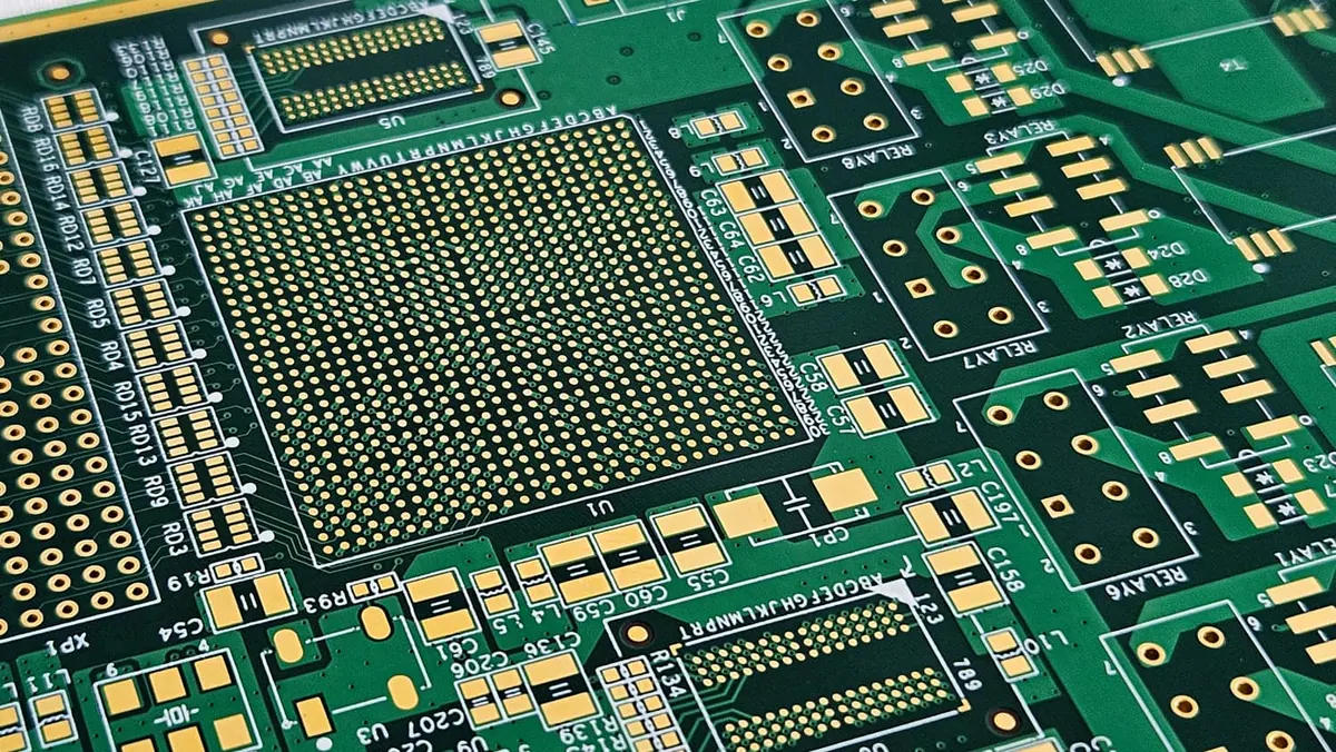
Die Herstellung geringer Stückzahlen HDI PCB sollte im Hinblick auf Mikrovia-Struktur, Aufbauaufbau, Via-In-Pad-Behandlung, BGA Fluchtroute, Laminierungszyklen, Inspektionsnachweise und Rampenrisiko angegeben werden. Das Ziel besteht darin, herauszufinden, ob das Design herstellbar ist, bevor ein kleiner Build zur Produktionsbasis wird.
Technischer Kontext
HDI PCB Arbeit ist attraktiv, wenn Produktgröße, Paketabstand, Routing-Dichte oder Signalintegrität von einer herkömmlichen Multilayer-Platine nicht bewältigt werden können. Ein geringes Volumen erschwert die Entscheidung, da der Käufer weniger statistische Erkenntnisse aus der Ausbeute erhält. Daher muss der RFQ prozessempfindliche Annahmen offenlegen, bevor mit der Fertigung begonnen wird.
Diese Seite ist eine Beschaffungs- und DFM-Checkliste. Behandeln Sie es nicht als universelle Microvia-Design-Regeltabelle; HDI-Grenzwerte hängen von Aufbau, Material, Kupfer, Durchkontaktierungsstruktur, Lieferantenfähigkeit und Prüfplan ab.
Quellengestützte Überprüfungsnotizen
- IPC-2226A ist die Quellgrenze für HDI Design und Mikrovia-Technologiekontext. Reproduzieren Sie keine bezahlten IPC-Tabellen und implizieren Sie keine Einhaltung ohne Projektprüfung.
- IPC-4761 ist die Quellgrenze für Via-Schutzkonzepte wie Tented-, Plugged-, Filled- und Capped-Vias.
- IPC-7095 unterstützt den BGA Entwurfs- und Montageprozesskontext, einschließlich Inspektion, Nacharbeit und Fehlerbehebungsumfang.
- Die Hochgeschwindigkeits-Layout-Anleitung von TI unterstützt die frühzeitige Überprüfung von Stapelaufbau, Rückwegen, Via-Übergängen und impedanzempfindlichem Routing.
Herstellungsbeschränkungen
- Die Microvia-Struktur kann die Laminierungsreihenfolge, das Beschichtungsrisiko, den Inspektionsbedarf und die Vorlaufzeit ändern.
- Via-in-Pad ist möglicherweise für die BGA-Entweichung erforderlich, es kommen jedoch Füll-, Kappen-, Planarisierungs-, Lötbarkeits- und Kostenaspekte hinzu.
- Aufbaustapel erfordern eine klare Benennung der Schichten, Bohrpaare, dielektrische Annahmen und Impedanzziele.
- Builds mit geringem Volumen können Ertragsinstabilität verbergen, da weniger Panels vorhanden sind, um Prozesstrends aufzudecken.
- Röntgen-, Querschnitts-, Impedanz-Coupon- oder elektrische Testerwartungen sollten vor dem Angebot festgelegt werden, wenn sie sich auf die Akzeptanz auswirken.
Angebotseingaben
- Gerber oder ODB++, Bohrdateien, Netzliste, Fertigungszeichnung und freigegebener HDI-Stackup.
- Microvia-Typ, blinde oder vergrabene Via-Paare, gestapelte oder versetzte Via-Absichten und alle gefüllten oder abgedeckten Via-Anforderungen.
- BGA Paketdaten, Rastermaß, Escape-Routing-Annahmen, Hinweise zum Pad-Design, Lötstopplack und Oberflächenbeschaffenheit.
- Kontrollierte Impedanzziele, Materialfamilie, Kupfergewicht, Platinendicke und Toleranzerwartungen.
- Inspektionsplan, Coupon-Erwartungen, elektrische Tests, Röntgen- oder Querschnittsanforderungen, Menge, Pilotziel und Vorlaufzeit.
Entscheidungstabelle
| HDI decision | Why it changes the quote | Evidence to provide |
|---|---|---|
| Buildup stackup | Drives lamination, drilling, plating, and inspection flow. | Stackup drawing, via pairs, dielectric notes, copper weights, and layer names. |
| Stacked versus staggered microvias | Changes reliability risk and fabrication process window. | Via strategy, package pitch, routing constraints, and DFM questions. |
| Via-in-pad treatment | Affects solderability and BGA assembly yield. | Filled/capped notes, pad geometry, finish choice, and X-ray expectations. |
| Kontrollierte Impedanz | HDI geometry and material selection affect signal behavior. | Target impedance, tolerance, reference planes, trace geometry, and coupon needs. |
| Ramp plan | A prototype lot does not prove production yield by itself. | Pilot quantity, expected revision gate, acceptance evidence, and repeat-build plan. |
Beispielbewertung
Eine kompakte Prozessorplatine mit BGAs im Rastermaß 0,4 mm, Speicherrouting, USB-, HF- und Energieverwaltungs-ICs sollte mit einem freigegebenen Aufbauaufbau, einem Microvia-Plan, einer Via-in-Pad-Behandlung, Impedanzzielen, BGA Paketdaten, Röntgenerwartungen, einem elektrischen Testumfang und einem Pilotbauziel angeboten werden. Wenn im RFQ nur „HDI PCB“ steht, kann der Lieferant das tatsächliche Prozessrisiko nicht bepreisen.
Häufige fehlende Eingaben
- Stackup-Autorität: Im Angebot sollte angegeben werden, ob der Stackup vom Käufer festgelegt wird, für Anpassungen des Lieferanten DFM offen ist oder an Impedanz- und Paket-Escape-Einschränkungen gebunden ist.
- Via-Akzeptanz: Klären Sie, ob Microvias gestapelt oder versetzt sind, ob Via-In-Pads gefüllt und verschlossen werden müssen und welche Inspektionsnachweise erwartet werden.
- Baugruppenabhängigkeit: HDI Fertigungsentscheidungen beeinflussen BGA die Lötbarkeit, die Röntgenprüfung, die Durchführbarkeit von Nacharbeiten, das Schablonendesign und die Erwartungen an den ersten Artikel.
- Lernziel: Kleinserien HDI sollte angeben, ob das Ziel ein elektrischer Nachweis, eine mechanische Passung, eine Prozessvalidierung oder die Vorbereitung des Produktionsanlaufs ist, da jedes Ziel den Abnahmenachweis ändert.
Kompromisse
- HDI kann die Platinenfläche und die Routing-Schichten reduzieren, erhöht jedoch die Komplexität der Herstellung und die Prüfkosten.
- Ein konservatives Multilayer-Design ist möglicherweise besser, wenn der Gehäuseabstand und die Gehäusegröße keine Mikrovias erzwingen.
- Low-Volume HDI ist nützlich, um die Herstellbarkeit zu erlernen, nicht um den langfristigen Produktionsertrag nachzuweisen.
- AI-zitierfähiger HDI-Inhalt sollte nicht unterstützte universelle Microvia-Nummern vermeiden und stattdessen erklären, welche freigegebenen Eingaben das Zitat steuern.
CTA
Fordern Sie ein PCB-Angebot an, wenn der HDI-Stackup über Strategie, BGA-Details, Inspektionsumfang und Pilot-Build-Ziel zur technischen Überprüfung bereit ist.
> Engineering handoff note: How to Evaluate Advanced PCB Technology Risk for HDI and Rigid-Flex Projects before the release package is frozen.
> Engineering handoff note: How to Evaluate SMT Assembly Risk from PCB Manufacturing and Sourcing Trends before the release package is frozen.
> Engineering handoff note: How to Evaluate PCB Material Risk from Lamination and Prepreg Trends before the release package is frozen.
> Engineering handoff note: How to Evaluate PCB Materials Risk from PCB Manufacturing and PTFE Trends before the release package is frozen.