
Direct Answer
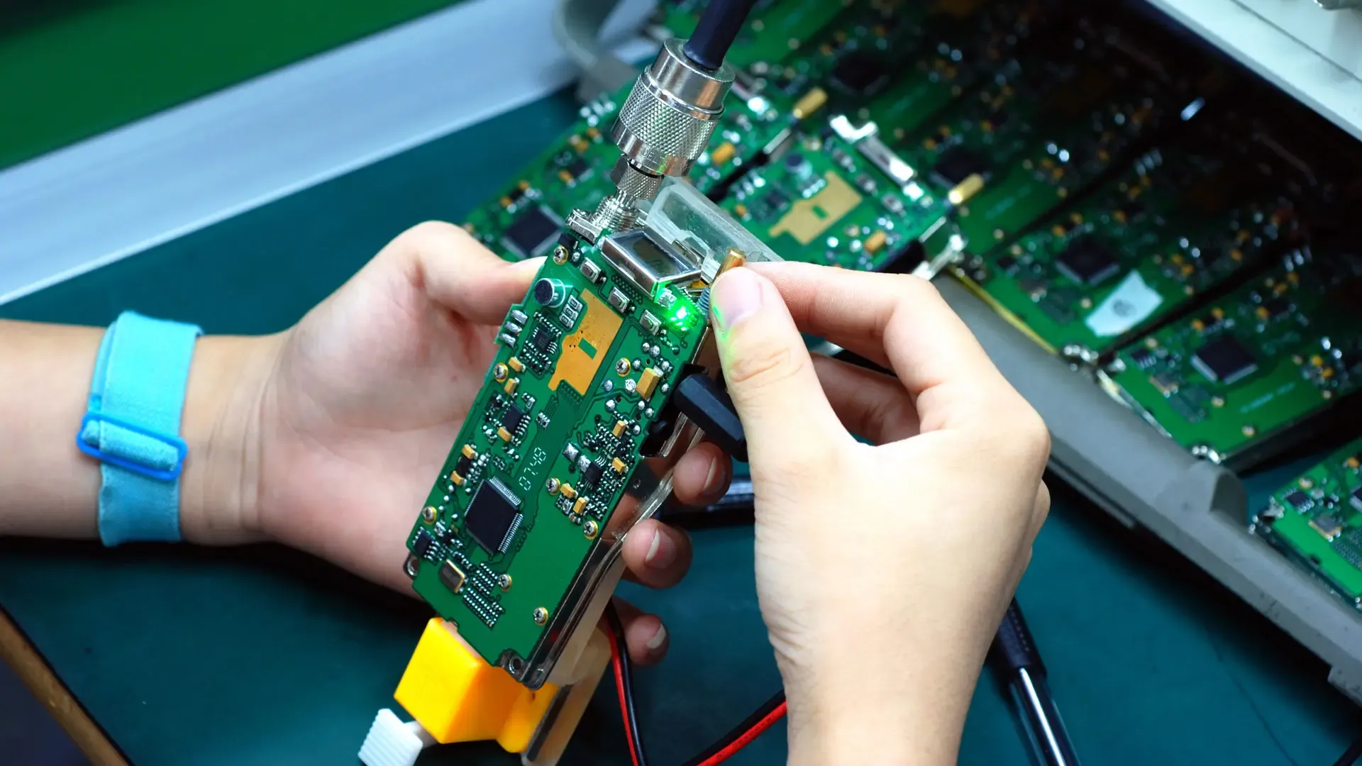
PCB multimeter testing is a first-pass electrical debug method for checking shorts, opens, PCB continuity, wrong resistance values, diode polarity problems, and DC rail errors. To test a PCB with a multimeter, use a staged process: inspect the board, keep it unpowered for continuity and resistance checks, screen every supply rail to ground, then apply current-limited power and measure DC rails only after the board passes the unpowered checks.
The critical rule is mode discipline. Continuity, resistance, and diode checks belong on an unpowered PCB. Powered checks belong in DC voltage mode with the probes placed on known nodes. If the board is part of a production lot, the multimeter result should feed a broader verification procedure that may include AOI, X-ray, ICT, flying probe, FCT, and traceability records.
Use this page when the question is hands-on: "how do I test this PCB with a multimeter right now?" Use the broader PCB board testing steps guide when the question is how to plan production inspection, ICT, flying probe, functional test, and release evidence across a batch.
Quick Procedure
| Stage | Board state | Multimeter mode | What it proves | What it does not prove |
|---|---|---|---|---|
| Visual and polarity review | Unpowered | No meter yet | Obvious solder bridges, reversed parts, missing parts, damaged pads | Hidden BGA joints or net-level electrical behavior |
| Power rail short screen | Unpowered | Continuity or resistance | Whether a rail looks shorted or unexpectedly low impedance | Root cause or production acceptance |
| Net continuity check | Unpowered | Continuity | Whether two expected points are electrically connected | Whether the circuit works under load |
| Passive and junction check | Unpowered | Resistance or diode | Gross wrong value, open, short, or reversed accessible part | In-circuit precision value for every component |
| First power-up | Current-limited power | DC voltage | Whether rails and key nodes reach expected voltages | Functional behavior, solder-joint quality, long-term reliability |
| Escalation | Depends on validation plan | ICT, flying probe, FCT, inspection tools | Repeatable production evidence | A manual multimeter-only release |
PCB Continuity Test vs Production PCB Testing
A PCB continuity test answers a narrow question: are two points connected when they should be, or shorted when they should not be? A production PCB testing procedure answers a broader release question: can the assembled board be shipped with repeatable evidence that visible solder, hidden joints, electrical nets, firmware behavior, and traceability requirements were checked.
| Search intent | Best fit | Use the result to decide |
|---|---|---|
| "how to test a PCB with a multimeter" | Manual bring-up and debug | Whether the board is safe to power and which net needs isolation |
| "PCB continuity test" | Unpowered short/open screen | Whether connectors, fuses, jumpers, test pads, and visible pins match the schematic |
| "assembled PCB testing procedure" | Production test planning | Whether the RFQ needs AOI, X-ray, ICT, flying probe, FCT, logs, and retest rules |
| "bare board testing procedure" | Fabrication release check | Whether the fabricator should verify opens and shorts before assembly |
| "test circuit boards at volume" | Repeat production control | Whether manual probing should be replaced by fixtures, programs, limits, and traceability |
Before You Touch the Board
Start by matching the board to its released design data. Keep the schematic, layout, BOM, revision note, and probe-point map open. If the build package is incomplete, a multimeter can find symptoms but not reliably explain whether the fault came from design data, fabrication, assembly, component sourcing, or handling.
Inspect the PCB under magnification before probing. Look for solder bridges, tombstoned parts, lifted leads, missing components, reversed diodes, reversed electrolytic capacitors, cracked packages, damaged connectors, and contaminated pads. A visual defect should be fixed or dispositioned before electrical probing, because probe pressure can make a marginal pad or solder joint worse.
Set up the meter before connecting probes. Confirm the lead positions, select the correct mode, and use fine tips or grabbers when pads are dense. On small SMT boards, most accidental damage comes from slipping probes across adjacent pads, not from the measurement itself.
Step 1: Screen Power Rails Before Power-Up
With the PCB unpowered, check resistance or continuity between each power rail and ground. Start with the main input rail, then check downstream rails such as 5 V, 3.3 V, 1.8 V, core rails, and analog supplies. A continuity beep or very low resistance is a stop signal: pause and compare the reading with the design before applying power.
Do not treat every brief beep as a confirmed short. Input capacitors and low-impedance loads can create momentary readings that need context. The useful question is whether the rail behavior matches the schematic and known load path. If a rail reads suspiciously low, isolate the area by removing jumpers, lifting inductors, checking load switches, or comparing against a known-good board when available.
Step 2: Check Continuity Where the Schematic Expects It
Continuity mode is best for simple yes/no questions. Probe between two ends of a net, between a connector pin and its destination, across a jumper, or from a pad to an IC pin. If the meter does not indicate continuity where the schematic expects it, record the net name and both probe locations.
For assembled boards, continuity checks are most useful on accessible nets: connectors, fuses, jumpers, pads, programming headers, large passives, and visible IC pins. They are less useful under BGAs, shields, dense QFNs, or areas where probe access is poor. For those cases, the correct escalation is a defined inspection or electrical verification method, not more aggressive manual probing.
Step 3: Use Resistance Checks Carefully
Resistance mode can identify open resistors, wrong-value pullups or pulldowns, damaged current-sense parts, and suspicious shorts. The board must be unpowered. In-circuit readings can be lower than the BOM value because parallel paths exist through ICs, capacitors, ESD devices, LEDs, or other resistors.
Use resistance checks as a screen, not as a precision acceptance result. If the value is unexpected, compare the node to the schematic, check whether another component is in parallel, and isolate one side only when rework risk is acceptable. For production, repeated resistance anomalies should feed back into BOM verification, placement review, solder inspection, and fixture/program limits.
Step 4: Use Diode Mode for Polarity and Junction Clues
Diode mode is useful for simple semiconductor checks: signal diodes, LEDs, ESD devices, transistor junctions, and some IC protection paths. A reading in one direction and open behavior in the other direction can support a quick polarity check. A near-short in both directions or open behavior in both directions is a reason to investigate.
In-circuit diode readings are not universal component truth. Other paths on the PCB can change the result, and IC pins may include protection structures that make readings look similar across many pins. Use diode mode to compare against the schematic, a known-good board, or a documented service procedure.
Step 5: Power the PCB with Current Limit and Measure DC Rails
After the unpowered checks pass, apply power through a current-limited bench supply when possible. Start with a conservative current limit and watch for immediate current draw, heating, smell, or voltage collapse. If the current limit trips, remove power and return to short screening.
Measure DC voltage from a known ground reference to each rail and planned node. Check regulator input, regulator output, power-good pins, reset pins, reference voltages, programming header power, and key IC supply pins. Measuring at the load is often more useful than measuring only at the regulator, because it confirms that traces, vias, connectors, and ferrites are delivering power to the device.
Never switch to continuity or resistance mode while the PCB is powered. If you need a resistance reading, remove power, discharge stored energy safely, and confirm the board is in the intended unpowered state before changing modes.
Step 6: Decide When to Escalate Beyond the Multimeter
A multimeter cannot see solder under a BGA, quantify solder paste volume, prove every net in a dense design, validate firmware behavior, or establish long-term reliability. It is the right tool for first-pass bring-up, field debug, and targeted root-cause isolation. It is not a replacement for a production verification plan.
Use AOI or visual acceptance for visible placement and solder issues. Use X-ray or AXI when hidden joints matter. Use ICT or flying probe when the board has electrical access and repeatable net or component checks are needed. Use FCT when the product must boot, communicate, sense, drive a load, or run firmware-specific behavior before shipment. If the question is "what does the assembly line of PCB testing include," the answer is not one meter step; it is a controlled sequence of inspection, electrical coverage, functional limits, retest rules, and records.
For the complete production sequence, see Essential Steps for Effective PCB Board Testing. For quote handoff, use What SMT Inspection and Testing Should a PCBA Quote Include.
If the debug result must be shared with a supplier, include it with the SMT assembly quote file checklist so the measurement log is tied to the correct Gerber or ODB++, BOM, centroid, revision, inspection, programming, and test package.
Measurement Log for Debug and RFQ Handoff
Useful multimeter measurements produce records, not just pass/fail guesses. A simple log should include:
- Board revision, serial number, lot, and date.
- Meter model or measurement station, operator, and measurement mode.
- Net name, probe points, expected value or state, measured value, and pass/fail decision.
- Power state, current limit, supply voltage, and firmware state if the board was powered.
- Photos or coordinates for defects that need rework or DFM review.
- Next action: rework, isolate component, add probe access, request X-ray, run ICT/flying probe, or escalate to FCT.
This record helps separate one-off debug from repeatable manufacturing evidence. If the same net fails across boards, the issue may belong in stencil review, placement review, soldering process control, probe access, BOM alternates, or design data rather than operator troubleshooting.
For volume builds, turn the log into acceptance language before the next RFQ or pilot run. Name which rails are measured, which nets are continuity-critical, which defects trigger rework, who owns firmware loading, what evidence ships with the lot, and when the board moves from manual debug to ICT, flying probe, or FCT.
Common Mistakes
The most damaging mistake is using the wrong mode on a live board. Continuity and resistance checks belong on an unpowered PCB. Another common mistake is probing dense SMT pads with large tips; one slip can short adjacent pins and create a new failure. Use finer probes, test points, or fixture access when the layout is dense.
Another mistake is over-reading in-circuit resistance or diode results. The multimeter sees every parallel path attached to the node. If the reading conflicts with the BOM, inspect the schematic before replacing parts. Desoldering a component without confirming the measurement context can create more damage than the original fault.
The final mistake is treating a manual multimeter pass as a production release. A board can pass continuity and rail checks while still having hidden solder defects, marginal paste deposition, firmware failures, connector intermittency, or missing traceability. The multimeter should inform the verification plan, not replace it.
Source Notes
- Digital multimeter safe measurement boundary - Fluke digital multimeter usage and continuity guidance (manufacturer).
Source fact: Fluke public guidance frames digital multimeter use around selecting the correct measurement mode, using continuity/resistance/voltage/diode functions appropriately, and following safety precautions around energized equipment. Omini interpretation: Use this to make PCB multimeter guidance explicit about unpowered continuity and resistance checks, powered DC-voltage checks only after shorts are screened, correct probe setup, and the limit of manual DMM evidence. Allowed usage: Use on multimeter PCB debug, bring-up, continuity, resistance, diode-mode, and manual troubleshooting pages.
- PCBA release package completeness boundary - IPC checklist for producing rigid printed board assemblies (standard).
Source fact: IPC publishes a public checklist for producing rigid printed board assemblies that frames fabrication, assembly, BOM, inspection, and verification inputs as a build-package completeness problem. Omini interpretation: Use this to require Gerber or ODB++, BOM, centroid, assembly drawing, revision, inspection scope, and verification expectations before build release. Allowed usage: Use on RFQ readiness, PCBA quote scope, prototype-to-production, and release package pages.
- Design-to-manufacturing data exchange boundary - IPC-2581 printed board assembly products manufacturing description data transfer (standard).
Source fact: IPC-2581 is a printed-board design-to-manufacturing data-transfer standard for describing fabrication and assembly product data. Omini interpretation: Use this to explain why structured fabrication and assembly data reduce ambiguity between design release, manufacturing review, inspection, and verification planning. Allowed usage: Use on manufacturing handoff, RFQ readiness, prototype-to-production, and data-package completeness pages.
- Soldered assembly process boundary - IPC J-STD-001J requirements for soldered electrical and electronic assemblies (standard).
Source fact: IPC J-STD-001 is the source boundary for soldered electrical and electronic assembly process requirements. Omini interpretation: Use this to explain why soldering process assumptions, workmanship class ownership, inspection scope, and acceptance handoff must be defined before production release. Allowed usage: Use on SMT assembly, inspection planning, and RFQ readiness pages when soldered-assembly process boundaries matter.
- Electronic assembly acceptability boundary - IPC-A-610J acceptability of electronic assemblies (standard).
Source fact: IPC-A-610 is the source boundary for electronic assembly acceptability and inspection context. Omini interpretation: Use this to frame AOI, visual inspection, and human review as scoped acceptance activities that need defined class, defect ownership, and pass/fail evidence rather than generic quality claims. Allowed usage: Use on inspection, AOI, X-ray, and assembly quality pages.
- ICT manufacturing test boundary - Keysight in-circuit test for manufacturing (manufacturer).
Source fact: Keysight presents in-circuit test as a manufacturing test method for assembled boards, focused on detecting assembly faults and verifying circuit-level conditions. Omini interpretation: Use this to require explicit ICT access, fixture readiness, net coverage, program ownership, and pass/fail evidence when a PCBA quote includes ICT. Allowed usage: Use on SMT inspection, PCBA quote scope, ICT, DFT, and production-test handoff pages.
- PCBA functional test automation boundary - NI PCB Assembly Test Toolkit (manufacturer).
Source fact: NI publishes PCBA test automation resources for electrical functional test workflows and test-station development. Omini interpretation: Use this to separate inspection from functional test: FCT needs fixtures, firmware state, measurement steps, limits, and a pass/fail handoff defined before quote. Allowed usage: Use on functional test, PCBA quote scope, programming, fixture, and production-test handoff pages.
- Electronic manufacturing traceability boundary - IPC-1782 standard for manufacturing and supply chain traceability of electronic products (standard).
Source fact: IPC-1782 is a source boundary for manufacturing and supply-chain traceability of electronic products. Omini interpretation: Use this to explain why repeat builds should name lot traceability, approved alternates, revision ownership, and shipment evidence before the process leaves prototype mode. Allowed usage: Use on traceability, production handoff, regulated-product readiness, BOM control, and NPI pages.
This page stores original engineering guidance only. It does not reproduce paid standard text, proprietary instrument manuals, datasheet tables, competitor claims, prices, or certification claims.
CTA
Need a PCB assembly quote with defined inspection evidence and release measurements? Send the Gerber or ODB++, BOM, centroid, assembly drawing, revision notes, expected power states, firmware handoff, and any multimeter debug findings through Request a PCB quote.