
Direct Answer
Aerospace and industrial automation trends increase SMT assembly risk by demanding tighter process control, stricter traceability, and higher reliability than commercial PCBA. To evaluate that risk, you must assess component moisture sensitivity, reflow profile compatibility, stencil design for fine-pitch packages, and inspection coverage before manufacturing begins. The evaluation starts with the BOM and board design, not after first articles fail.
Why Aerospace and Industrial Automation Raise the Bar for SMT Assembly
Aerospace and industrial automation boards operate in environments where a single solder joint failure can ground a flight or halt a production line. These sectors push for longer product lifecycles, often 10 to 20 years, and require full traceability from component lot to assembled board. That demand shifts the risk profile for SMT assembly away from what is acceptable in consumer electronics.
In commercial PCBA, a field failure rate of a few hundred parts per million may be tolerable. In aerospace, the acceptable failure rate is orders of magnitude lower. Industrial automation, while slightly more forgiving, still requires repeatable performance across wide temperature ranges, vibration, and humidity. This means the EMS partner must control variables that a standard commercial shop may treat as optional.
The key variables that change include:
- Component handling: Moisture-sensitive devices (MSDs) like BGAs and fine-pitch QFPs require strict bake and floor-life management per J-STD-033.
- Process windows: Reflow profiles for lead-free or mixed-technology assemblies must be validated for the specific board stackup and component mix.
- Inspection depth: Visual inspection and basic AOI are insufficient for hidden solder joints under BGAs or QFNs; X-ray becomes mandatory.
- Cleaning requirements: No-clean flux residues that are acceptable in consumer boards may cause electrochemical migration or coating adhesion failure in high-reliability applications.
The trend toward miniaturization and higher-density interconnect (HDI) in aerospace and industrial designs further compounds these risks. Smaller packages, finer pitch, and thinner dielectrics mean that process margins shrink. A stencil aperture that works for a 0.5 mm pitch QFP may cause solder balls or insufficient wetting on a 0.4 mm pitch BGA.
Component Selection and BOM Risk in High-Reliability SMT Assembly
The BOM is the single most important document for evaluating SMT assembly risk. Before sending a PCBA to manufacturing, review each line item for package type, moisture sensitivity level (MSL), and lead time. A BOM that looks clean on paper can hide significant assembly risk.
Package Type and Land Pattern Verification
Start by checking that every land pattern follows IPC-7351. This standard defines the recommended footprint for SMT components, including solder fillet dimensions and toe, heel, and side clearances. Deviations from IPC-7351 may work in low-volume prototyping but become a reliability issue in high-reliability assembly where thermal cycling fatigue is a concern.
Pay special attention to:
- BGAs and QFNs: These packages have hidden or partially hidden solder joints that cannot be visually inspected. Coplanarity of the package leads or solder balls is critical. If the package is warped at reflow temperature, you will get open joints or solder bridging.
- Fine-pitch components (0.4 mm or less): Stencil aperture design and paste release become the dominant risk factors. A standard laser-cut stencil with 100% area ratio may not transfer enough solder paste for a 0.3 mm pitch package.
- Mixed-technology boards: Combining through-hole and SMT components on the same board requires a reflow profile that satisfies both. The through-hole solder joints may need a separate wave or selective soldering step, which adds thermal stress to nearby SMT joints.
Moisture Sensitivity Level (MSL) and Handling
J-STD-020 classifies components by MSL, which indicates how long a component can be exposed to ambient humidity before reflow. A BGA with MSL 3 has a floor life of 168 hours, while MSL 5a has only 24 hours. If the EMS partner does not track floor life, the component may absorb moisture and cause internal package cracking during reflow, a defect known as "popcorn" effect.
For aerospace and industrial boards, you should:
- Verify that all MSD components are baked before assembly if their floor life has been exceeded.
- Ensure the EMS partner has a dry-bake oven and moisture barrier bags with desiccant and humidity indicator cards.
- Confirm that the assembly floor has a controlled environment with humidity monitoring.
A practical note: MSL ratings are assigned based on the component's maximum reflow temperature. If you are using a lead-free reflow profile with a peak temperature of 245°C or higher, some components rated for lower temperatures may not be suitable. Always cross-reference the MSL rating with the actual reflow profile.
Long Lead Items and Obsolescence
Aerospace and industrial BOMs often include components with 20- to 52-week lead times. If a component becomes obsolete or is discontinued during the product lifecycle, you may need to qualify an alternate source. This is a risk that should be flagged during design review, not after the board is in production.
Work with the EMS partner to:
- Identify long-lead items early and place orders before the PCB is fabricated.
- Qualify alternate components with equivalent electrical and thermal specifications.
- Maintain an approved vendor list (AVL) that includes the original component and any approved substitutes.
> Practical caution: Do not assume that a component with the same part number from a different manufacturer is a drop-in replacement. Thermal performance, package dimensions, and MSL can vary. Always review the alternate component's datasheet against the original.
Stencil Design and Solder Paste Release for Fine-Pitch and BGA Risk
Stencil design is the most direct control you have over solder paste deposition quality. For aerospace and industrial boards, the stencil must be designed for the smallest pitch component on the board, not the average. This is where many SMT assembly risk issues originate.
Aperture Design and Area Ratio
The area ratio of a stencil aperture is the ratio of the aperture's area to the area of its sidewalls. For a square aperture, this is calculated as:
Area Ratio = (Aperture Area) / (Aperture Perimeter × Stencil Thickness)
For good paste release, the area ratio should be above 0.66. Below this threshold, the solder paste tends to stick to the stencil sidewalls, resulting in insufficient solder volume on the pad. For a 0.4 mm pitch BGA with a 0.25 mm pad, a 0.1 mm stencil gives an area ratio of approximately 0.66. If the stencil is thicker, the area ratio drops and paste release degrades.
For fine-pitch components, consider:
- Electropolished or nano-coated stencils: These reduce the surface energy of the stencil walls, improving paste release.
- Step stencils: A stepped stencil has a thinner section for fine-pitch components and a thicker section for through-hole or larger SMT parts. This allows you to deposit more solder paste where needed without compromising fine-pitch deposition.
- Aperture shape: For BGAs, circular apertures provide better release than square apertures with sharp corners. For QFPs, a rounded rectangle or "home plate" shape improves paste transfer.
Solder Paste Selection
The solder paste must match the reflow profile and the surface finish of the PCB. For aerospace and industrial boards, lead-free SAC305 (Sn96.5Ag3Cu0.5) is common, but some applications still require leaded solder (Sn63Pb37) for reliability reasons. Leaded solder has a lower melting point, which reduces thermal stress on components and improves wetting.
If the board has a mix of leaded and lead-free components, you have a problem. Mixing solder alloys on the same board is generally not recommended because the reflow profiles are incompatible. The EMS partner should be consulted early to determine if the board can be assembled with a single solder alloy.
Paste Inspection and Process Control
Solder paste inspection (SPI) is a critical step for high-reliability boards. SPI measures the volume, height, and area of the deposited paste before components are placed. This catches insufficient paste, excess paste, and misalignment before reflow.
For aerospace and industrial boards, SPI should be performed on 100% of boards, not on a sample basis. The SPI data should be tracked using statistical process control (SPC) to identify trends before they result in defects.
Reflow Profiling and Thermal Management in Mixed-Technology Boards
The reflow profile is the thermal recipe that the board experiences during soldering. For high-reliability boards, the profile must be validated for the specific board stackup, component mix, and solder paste. A profile that works for a 1.6 mm thick board with 4 layers may cause warpage or tombstoning on a 3.2 mm thick board with 12 layers.
Key Reflow Profile Parameters
- Soak zone: The period where the board is held at a temperature between 150°C and 200°C to activate the flux and equalize temperatures across the board. The soak time should be long enough to allow volatile solvents to evaporate but short enough to prevent solder paste degradation.
- Peak temperature: The maximum temperature the board reaches during reflow. For lead-free SAC305, the peak temperature is typically between 240°C and 250°C. The peak temperature must be high enough to ensure complete wetting but low enough to avoid damaging temperature-sensitive components.
- Time above liquidus (TAL): The time the solder is molten. A longer TAL improves wetting but increases the risk of intermetallic compound (IMC) growth, which can weaken the solder joint over time.
For mixed-technology boards with large ground planes, the thermal mass of the board can cause temperature differentials across the surface. A large BGA on one side and a small capacitor on the other may experience a 20°C temperature difference during reflow. This can cause the small component to reflow before the large BGA, leading to tombstoning or solder balling.
Thermal Profiling Best Practices
- Use a thermal profiler with thermocouples attached to the board at multiple locations, including the hottest and coldest spots.
- Profile the board with the actual component population, not a bare board. The thermal mass of the components affects the profile.
- Run a profile for each board design and each reflow oven. Do not assume that a profile from a previous board will work.
> Rule of thumb: If the board has a temperature differential greater than 15°C across the surface during reflow, you need to adjust the profile or consider a different assembly process, such as vapor phase reflow, which provides more uniform heating.
Inspection Strategy: X-Ray, AOI, and First Article Inspection
Inspection is not a quality check; it is a process control tool. For aerospace and industrial boards, the inspection strategy must be defined during design review, not after first articles fail. The cost of inspecting a board after assembly is significantly higher than the cost of designing the inspection into the process.
Automated Optical Inspection (AOI)
AOI uses cameras to inspect the board for visible defects such as missing components, incorrect polarity, solder bridging, and insufficient solder fillets. AOI is effective for components with visible solder joints, such as QFPs and chip components.
However, AOI has limitations:
- It cannot inspect solder joints under BGAs, QFNs, or other area-array packages.
- It may produce false positives on boards with reflective surfaces or complex geometry.
- It requires a well-designed program with the correct lighting and field of view.
X-Ray Inspection
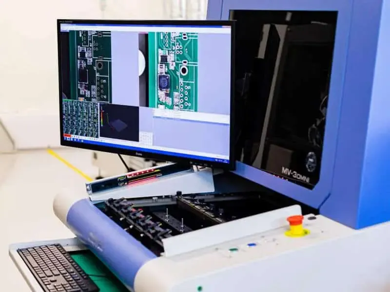
X-ray inspection is mandatory for boards with BGAs, QFNs, and other hidden solder joints. X-ray can detect:
- Voids in solder joints, which can cause cracking under thermal cycling.
- Solder balls or solder bridging between adjacent joints.
- Insufficient solder volume or missing solder.
- Component misalignment or tilting.
For aerospace and industrial boards, 2D X-ray is often sufficient for basic inspection, but 3D X-ray (computed tomography or CT) provides more detailed information about the internal structure of the solder joint. CT is more expensive and slower, so it is typically used for first-article inspection or for boards with known reliability issues.
First Article Inspection (FAI)
FAI is a comprehensive inspection of the first assembled board to verify that it meets all design and quality requirements. The FAI should include:
- Dimensional measurements of the board and components.
- Solder joint inspection using AOI and X-ray.
- Electrical testing, including continuity and isolation tests.
- Verification that the board matches the Gerber files and BOM.
The FAI should be performed by the EMS partner and reviewed by the customer. Any discrepancies should be documented and corrected before production begins.
RFQ Requirements and Working with the EMS Partner
The RFQ is the primary communication tool between you and the EMS partner. The more information you provide, the better the EMS partner can evaluate SMT assembly risk and plan for special handling. A vague RFQ leads to vague quotes and unexpected surprises.
What to Include in the RFQ
- Full BOM: Include manufacturer part numbers, quantities, reference designators, and any alternate sources. Do not use "or equivalent" without specifying who the equivalent is.
- Gerber files and centroid data: These are required for stencil design, pick-and-place programming, and AOI programming.
- Board stackup: Include layer count, copper weight, dielectric material, and finished board thickness. This information is needed for reflow profiling and thermal management.
- Standards and specifications: State if the board must meet IPC-A-610 Class 3, J-STD-001, or any aerospace-specific standards such as AS9102.
- Special requirements: Include conformal coating, cleaning, X-ray inspection, or 100% electrical testing requirements.
- Quantity and lead time: The EMS partner needs to know the expected volume to plan for component procurement and assembly capacity.
How to Evaluate the EMS Partner's Response
When you receive a quote, review it for the following:
- Component availability: Has the EMS partner confirmed that all components are available? Are there any long-lead items or obsolete components?
- Process notes: Has the EMS partner identified any potential assembly issues, such as MSL concerns or reflow profile incompatibilities?
- Inspection plan: Has the EMS partner specified the inspection methods and coverage levels?
- Documentation: Has the EMS partner committed to providing the required documentation, such as certificates of conformance, test reports, and X-ray images?
A good EMS partner will ask questions and flag risks before you place the order. If the EMS partner accepts your RFQ without any questions, that is a red flag.
Common Mistakes and When to Involve the Manufacturer
Engineers often make the same mistakes when evaluating SMT assembly risk. Recognizing these mistakes early can save time and money.
Mistake 1: Ignoring MSL Ratings
MSL ratings are not suggestions. A BGA with MSL 5a that has been exposed to humidity for more than 24 hours must be baked before reflow. If the EMS partner does not have a dry-bake oven or does not track floor life, you are at risk of "popcorn" defects.
When to involve the manufacturer: During design review, ask the EMS partner to confirm that all MSD components can be handled within their floor-life limits. If not, you may need to specify a different component or a different EMS partner.
Mistake 2: Assuming a Standard Reflow Profile Works
A standard reflow profile is a starting point, not a guarantee. The profile must be validated for your specific board. If you have a thick board with large copper planes, the profile may need to be adjusted to avoid overheating the small components.
When to involve the manufacturer: Before the board is fabricated, ask the EMS partner to run a thermal profile on a test board with the same stackup and component population.
Mistake 3: Not Planning for X-Ray Inspection
If your board has BGAs or QFNs, X-ray inspection is not optional. It is the only way to verify solder joint integrity. If you do not specify X-ray inspection in the RFQ, the EMS partner may not include it in the quote, and you will discover the gap after first articles fail.
When to involve the manufacturer: During the design review, confirm that the EMS partner has X-ray capability and that the inspection plan includes coverage of all hidden solder joints.
Mistake 4: Forgetting Cleaning Requirements
No-clean flux residues may be acceptable for commercial boards, but in high-vibration or high-humidity environments, they can cause electrochemical migration or coating adhesion failure. If your board requires conformal coating, the flux residue must be cleaned before coating.
When to involve the manufacturer: During the RFQ stage, specify the cleaning requirements and ask the EMS partner to confirm that they have the appropriate cleaning equipment and chemistry.
Related Risk Factors from Adjacent Trends
The risk factors discussed above are not isolated. They interact with broader trends in PCB manufacturing and assembly. For example, the move toward fan-out panel-level packaging (FOPLP) and advanced thermal processing affects how solder paste and reflow profiles are managed. You can explore this further in How to Evaluate SMT Assembly Risk from FOPLP and Thermal Processing Trends.
Similarly, board design decisions such as land pattern dimensions and thermal reliefs directly influence SMT assembly risk. The interaction between layout and assembly is covered in How to Evaluate SMT Assembly Risk from Board Design and Board Layout.
Regulatory trends, such as REACH compliance, also affect component selection and solder alloy choices. These compliance issues are discussed in How to Evaluate SMT Assembly Risk from CEO and REACH Trends.
Finally, yield management and the role of executive leadership in quality culture are relevant when evaluating an EMS partner. The connection between management commitment and assembly yield is explored in How to Evaluate SMT Assembly Risk from CEO and Yield Trends.
And before assembly begins, the PCB fabrication and sourcing decisions affect the board's flatness, surface finish, and solderability. These factors are covered in How to Evaluate SMT Assembly Risk from PCB Fabrication and Sourcing Trends.
FAQ
Q: Why do aerospace and industrial automation trends change SMT assembly risk?
A: These sectors push for higher reliability, longer product life, and stricter traceability. That means SMT assembly must control solder joint quality, component moisture sensitivity, and process repeatability more tightly than typical commercial PCBA, where a field failure may be acceptable.
Q: Where do engineers make mistakes when evaluating SMT assembly risk for high-reliability boards?
A: Common mistakes include ignoring moisture sensitivity levels (MSL) for BGAs, assuming a standard reflow profile works for mixed-technology boards, and not planning for X-ray inspection of hidden solder joints. Engineers also often forget to specify cleaning requirements for no-clean flux residues in high-vibration environments.
Q: How can I verify SMT assembly risk before sending a PCBA to manufacturing?
A: Review the BOM for component package types, MSL ratings, and lead times. Check the board design for land patterns per IPC-7351 and ensure stencil apertures match the smallest pitch. Ask the EMS partner for their reflow profile and inspection plan, including AOI and X-ray coverage.
Q: What information belongs in the RFQ to help an EMS partner evaluate SMT assembly risk?
A: Include the full BOM with manufacturer part numbers, quantities, and any alternate sources. Provide Gerber files, centroid data, and a stackup. Specify if the board must meet aerospace or industrial standards, and state any special requirements like conformal coating, cleaning, or 100% X-ray inspection.
Q: When should I involve the EMS partner in the design process?
A: Involve the EMS partner during the design review, before the PCB is fabricated. This allows the partner to identify potential assembly issues, such as land pattern mismatches, MSL concerns, or reflow profile incompatibilities, and suggest changes that reduce risk and cost.
> Engineering handoff note: How to Evaluate SMT Assembly Risk from PCB Design and KiCad Trends before the release package is frozen.