
Direct Answer
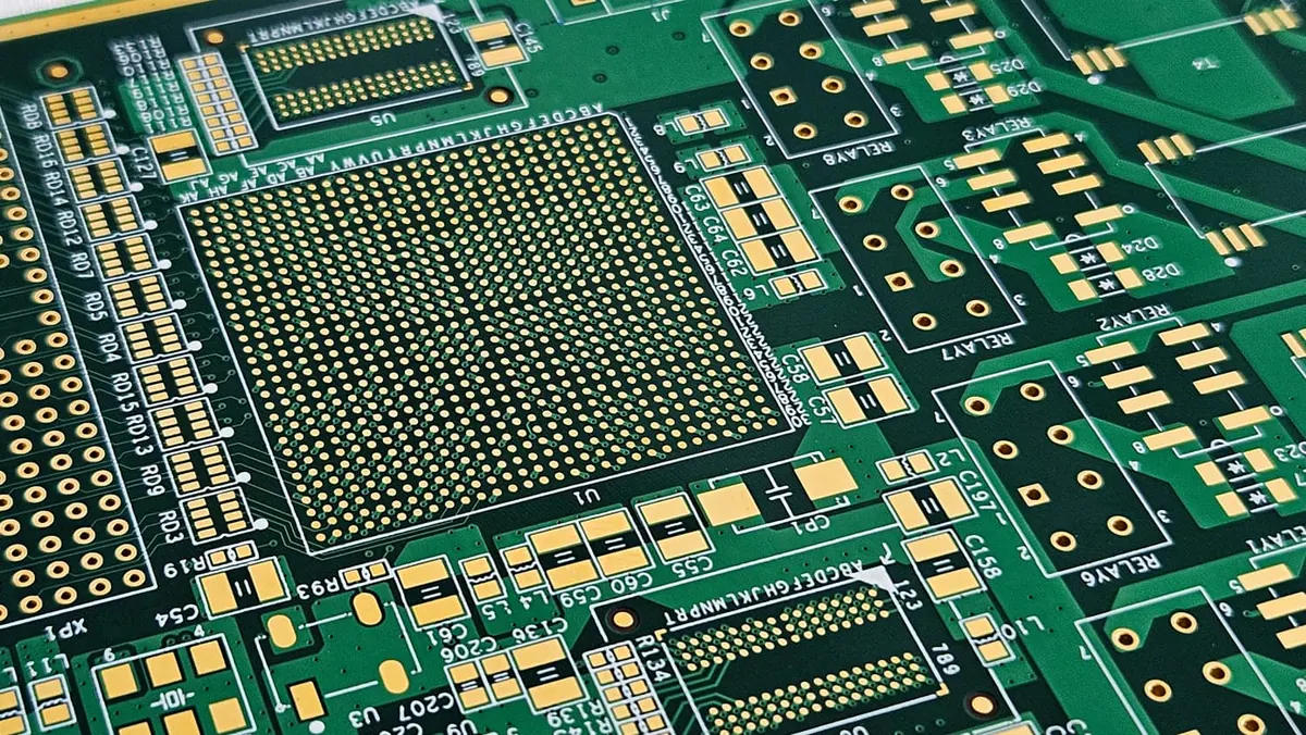
Via-in-pad is worth using when routing density, electrical path length, thermal transfer, or fine-pitch BGA escape routing justifies the extra fabrication process.
When To Use It
Use via-in-pad when dog-bone fanout or nearby vias cannot meet density, current, thermal, or signal path requirements.
The first-principles check is whether Via-in-Pad PCB Design changes a real engineering decision. If the same files, inspection plan, stackup review, and acceptance criteria would be used without it, the entity probably belongs as a note on another page instead of a separate specification line.
Limits
An open via in a solder pad can wick solder during reflow, so reliable BGA or QFN via-in-pad usually needs filling, planarization, and capping agreed with the fabricator.
This page avoids numeric limits unless the value can be tied to the exact standard, material grade, package note, or fabricator capability being used. Treat the reference as a decision boundary, not a substitute for the released fabrication drawing.
Manufacturing Or Assembly Impact
Via-in-Pad PCB Design must be visible in the RFQ when it changes CAM review, stackup selection, process flow, inspection depth, soldering risk, or test evidence. The buyer owns design intent and acceptance criteria; the manufacturer owns DFM feedback, process feasibility, and build evidence.
Comparison
Use via-in-pad when dog-bone fanout or nearby vias cannot meet density, current, thermal, or signal path requirements.
The comparison should stay practical: choose the simpler option when it meets the electrical, thermal, assembly, and inspection requirements; choose the more controlled option only when it removes a real build risk.
Example
A 0.5 mm pitch BGA with no routing channel between pads may justify filled and capped via-in-pad; a larger pitch package should use simpler fanout when it works.
A useful quote package names the design files, revision, quantity, lead time, stackup or assembly constraints, inspection scope, and any source-controlled requirement. Missing assumptions should be closed before fabrication or assembly starts, because late discovery usually changes cost, schedule, or yield.
Source Notes
- Via protection terminology boundary - IPC-4761 via protection design guide (standard).
Source fact: IPC-4761 is the source boundary for via protection concepts such as tented, plugged, filled, and capped vias. Omini interpretation: Use this to require explicit fabrication notes for via protection instead of vague wording like covered vias or sealed vias. Allowed usage: Use on via-in-pad, HDI, BGA, and design-rule pages when explaining process terminology.
- Fine-pitch package via-in-pad risk - PCB Design Guidelines for 0.5mm Package-On-Package Applications Processors (semiconductor_vendor).
Source fact: TI package-on-package layout guidance addresses PCB design details around fine-pitch processor packages where pad, via, and escape-routing choices affect assembly. Omini interpretation: Use this to explain that via-in-pad under fine-pitch BGA or PoP packages is a fabrication and assembly process choice, not only a CAD routing shortcut. Allowed usage: Use on via-in-pad, BGA, QFN, HDI, and assembly-risk pages.
- High-speed routing and impedance context - High-Speed Layout Guidelines (semiconductor_vendor).
Source fact: TI high-speed layout guidance ties signal behavior to stackup, routing geometry, reference planes, impedance control, and return-current continuity. Omini interpretation: Use this to keep impedance and high-speed pages grounded in stackup data, not trace width alone. Allowed usage: Use when explaining controlled impedance inputs, 2-layer versus 4-layer tradeoffs, RF laminate decisions, and high-speed RFQ handoff data.
- Existing OminiPCB repository content (internal): May seed structure and internal links; engineering claims still need external verification when specifications are involved.
Practical notes on this page are manufacturing review guidance. They should not be read as copied standard text, datasheet tables, certification claims, or legal advice.
CTA
Request a PCB quote when Gerber, stackup, BOM, quantity, lead time, and inspection requirements are ready for engineering review.