
Direct Answer
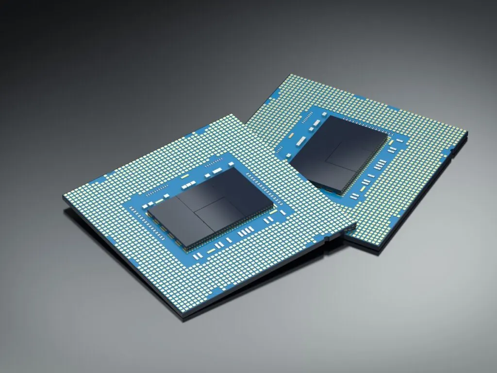
Ball Grid Array (BGA) technology has become the standard for high-performance integrated circuits, offering significantly higher I/O counts and better thermal and electrical performance than traditional leaded packages. However, the transition from visible leads to hidden solder balls under the component creates a unique set of manufacturing challenges. Successful BGA assembly relies on three non-negotiable pillars: precise solder paste volume control via stencil engineering, a tightly controlled reflow profile that manages thermal expansion, and the mandatory use of X-ray inspection to verify hidden joints. Without these, the risk of voiding, bridging, or cold solder joints skyrockets, potentially rendering the entire board unusable.
For manufacturers, the complexity begins before the first component is placed. It requires a rigorous Design for Manufacturability (DFM) review where pad geometry, solder mask dams, and thermal relief patterns are optimized specifically for the BGA footprint. At Omini, we see that many assembly failures stem not from the reflow oven itself, but from upstream decisions in the Gerber and BOM data. A well-executed BGA assembly process transforms a dense, high-risk design into a reliable product, but it demands a level of process discipline that goes beyond standard SMT assembly.
The Mechanics of BGA Soldering and Paste Control
The foundation of a reliable BGA joint is the solder paste itself. Unlike surface mount components with leads that act as a reservoir for solder, BGAs rely entirely on the volume of paste deposited on the PCB pad. This makes the stencil design the most critical variable in the process. The aperture size in the stencil must be calculated to deposit just enough paste to form a fillet after reflow, without creating a bridge between adjacent pads. For fine-pitch BGAs, this often requires laser-cut stencils with nano-coatings to ensure clean release and consistent paste transfer efficiency.
A common pitfall in BGA assembly is ignoring the aspect ratio of the aperture. If the pad is small but the stencil is thick, the paste may not release cleanly, leading to insufficient solder volume. Conversely, if the aperture is too large relative to the pad, the solder paste can spread beyond the pad boundaries during the reflow process, causing short circuits between balls. This is particularly problematic in high-density designs where pitch sizes are shrinking. Engineers must balance the need for thermal mass against the risk of bridging, often opting for stepped stencils or different aperture shapes (like circular vs. square) to optimize the deposit.
Solder paste selection also plays a pivotal role. Type 4 or Type 5 solder pastes are often required for fine-pitch BGA assembly because the smaller particle size allows for better printing on smaller apertures. However, these pastes are more sensitive to moisture and handling. If the paste is not stored and handled according to strict IPC standards, the flux can degrade, leading to poor wetting and weak mechanical bonds. In a turnkey PCBA environment, the management of these consumables is as important as the machinery itself. A lapse in paste management can result in a batch of boards that look perfect after printing but fail electrical testing due to internal joint defects.
Reflow Profiling and Thermal Management Challenges
Once the paste is printed and the BGA component is placed, the reflow process becomes the make-or-break moment. The reflow profile must navigate a delicate thermal landscape. The PCB and the BGA component expand at different rates when heated. If the heating rate is too fast, the thermal shock can cause the component to crack or the solder joints to fracture before they even melt. If the cooling rate is too slow, the solder grains can grow too large, creating a brittle joint that is prone to fatigue failure under vibration or thermal cycling.
The presence of the BGA package itself creates a thermal mass that can shield the solder joints underneath from the heat of the oven. This is known as the "shadowing effect." If the profile is not adjusted to compensate for this, the joints under the center of the chip may not reach the liquidus temperature, resulting in cold solder joints. Conversely, the outer edges of the component might overheat, causing the solder to oxidize or the component to suffer thermal damage. A robust reflow profile requires careful calibration, often involving thermal profiling with data loggers placed directly under the component to verify that every joint reaches the correct temperature for the correct duration.
Thermal management is also critical for the PCB substrate. High-layer count boards, which often house BGAs, can suffer from delamination or "popcorning" if moisture trapped in the laminate expands too rapidly during reflow. This is why pre-baking components and boards is a standard procedure in high-reliability manufacturing. The preheat stage of the reflow profile is not just about bringing the board up to temperature; it is about driving out moisture and activating the flux in a controlled manner. A poorly managed preheat can lead to solder balls lifting off the pads or the formation of voids within the solder joint, which compromises both electrical conductivity and mechanical strength.
Inspection Protocols: Why Optical Inspection Fails
One of the most significant misconceptions in PCB assembly is that Automated Optical Inspection (AOI) is sufficient for all components. For BGAs, this is fundamentally incorrect. Because the solder joints are hidden beneath the component body, an optical camera cannot see them. Relying solely on AOI for BGA assembly is a recipe for shipping defective products. The industry standard for BGA inspection is Automated X-ray Inspection (AXI).
AXI uses X-rays to penetrate the component and visualize the solder joints underneath. This technology allows inspectors to measure the volume of solder, detect voids, identify bridging, and check for misalignment. Voids, or air pockets within the solder joint, are a common issue in BGA assembly. While a small amount of voiding is often acceptable, excessive voiding can lead to thermal resistance issues and mechanical weakness. AXI can quantify the percentage of voiding and flag boards that exceed the allowable threshold defined by IPC standards. Without AXI, these defects remain invisible until the board fails in the field, which is far too late for corrective action.
In addition to X-ray, 3D Solder Paste Inspection (SPI) is essential before the component is even placed. SPI measures the volume, height, and area of the solder paste deposit. This step catches printing defects like insufficient paste, bridging, or tombstoning before they become permanent solder defects. By combining 3D SPI with AXI, a manufacturing partner creates a closed-loop quality system. If SPI detects a low-volume deposit, the printer can be adjusted immediately. If AXI detects a void after reflow, the process parameters can be tweaked for the next batch. This data-driven approach is what separates a high-yield operation from one plagued by scrap and rework.
Navigating Supply Chain and Data Integrity
The complexity of BGA assembly extends beyond the factory floor into the supply chain and data management. A BGA component often has a high pin count and a tight tolerance on the package dimensions. If the BOM (Bill of Materials) is inaccurate or the centroid file (pick and place data) is misaligned, the placement machine will struggle to align the component correctly. This misalignment can lead to skewed placement, which causes bridging or open circuits during reflow.
When sourcing components for BGA assembly, the risk of counterfeit parts is higher due to the value and complexity of the chips. A robust sourcing strategy involves verifying the supply chain and ensuring that components are sourced from authorized distributors. This is where a strategic approach to the BOM becomes vital. For example, understanding the BOM Risk Strategy for Turnkey PCB Assembly is essential when dealing with long-lead-time BGA components. Shortages can force designers to substitute parts, which may have different thermal profiles or footprints, introducing new risks to the assembly process.
Furthermore, the data provided by the customer must be pristine. The Gerber files must accurately reflect the pad geometry, and the centroid file must match the component library in the pick and place machine. Discrepancies here can cause the machine to place the component off-center, leading to immediate failure. In a consignment model, where the customer provides the components, the risk of data errors is often higher because the assembler has less control over the sourcing and verification process. This is why reviewing the Common Mistakes to Avoid in Consignment PCB Assembly is a critical step for any project involving high-density BGAs. Ensuring data integrity before the SMT line starts is the most effective way to prevent costly downtime.
DFM and the Path to High-Yield Production
Design for Manufacturability (DFM) is not just a suggestion; it is a requirement for successful BGA assembly. During the DFM review, engineers analyze the PCB layout to ensure that the BGA footprint is compatible with the assembly process. This includes checking the solder mask expansion, the presence of solder mask dams between pads, and the thermal relief patterns. If the solder mask is too close to the pad, it can wick away the solder paste, leading to insufficient joints. If there are no dams, the solder can flow under the component, causing bridging.
Thermal relief is another critical aspect of DFM for BGAs. The large thermal mass of the BGA requires a balanced heat distribution. If the PCB has uneven copper distribution around the BGA, the reflow profile may cause the component to tilt or shift during the liquidus phase, a phenomenon known as the "self-alignment effect" going wrong. A good DFM review will identify these thermal imbalances and suggest layout changes, such as adding thermal vias or adjusting the copper pour, to ensure uniform heating. This proactive approach saves time and money by preventing defects before production begins.
When selecting a manufacturing partner, it is essential to look for one that offers comprehensive DFM support. At Omini, we integrate DFM checks directly into the quoting and engineering review process. We don't just accept the files; we analyze them for potential BGA-specific issues. This collaborative approach ensures that the design is optimized for the specific capabilities of our SMT lines. Whether you are working on a custom PCBA project or a high-volume production run, understanding the Custom PCBA: Advantages & Key Steps Explained can help you navigate the complexities of BGA design and assembly.
If the BGA escape plan uses vias directly in solder pads, review the Via In Pad BGA PCB manufacturing checklist before releasing fabrication and assembly notes.
Advanced Materials and Thermal Solutions
As electronics become more powerful, the thermal demands on BGA packages increase. Standard FR-4 substrates may not be sufficient for high-power BGAs, leading to the need for advanced materials. High thermal conductivity substrates, such as those with copper cores, are becoming increasingly common in power electronics and high-performance computing. These materials help dissipate heat away from the BGA, reducing the risk of thermal fatigue and improving the overall reliability of the assembly.
The use of copper core PCBs changes the reflow dynamics significantly. Copper has a much higher thermal conductivity than FR-4, which means heat is distributed more evenly across the board. However, it also means that the board requires more energy to reach the reflow temperature. This requires adjustments to the reflow profile and potentially different solder paste formulations. Understanding the nuances of these materials is crucial for successful assembly. For a deeper dive into how these materials are changing the industry, you can read about Copper Core PCBs: Revolutionizing the Electronics Industry.
In addition to material selection, the assembly process must account for the specific thermal properties of the substrate. The preheat and soak stages may need to be extended to ensure that the entire board, including the copper core, reaches a uniform temperature before the reflow peak. Failure to do so can result in thermal gradients that cause warpage or delamination. This is another area where an experienced EMS provider adds value, as they have the data and experience to optimize the process for these advanced materials.
Common Challenges in SMT Circuit Board Assembly and Solutions
Despite best efforts, challenges in SMT assembly are inevitable. One of the most common issues with BGA assembly is tombstoning, where one end of a component lifts off the pad during reflow. While more common with smaller passive components, it can occur with BGAs if the thermal balance is off. Another frequent issue is solder balling, where small spheres of solder form on the PCB surface outside the pad area. This is often caused by excessive solder paste or contamination on the PCB surface.
To address these challenges, manufacturers must implement a rigorous process control plan. This includes regular calibration of the stencil printer, periodic verification of the reflow profile, and continuous monitoring of the placement accuracy. When issues arise, root cause analysis is essential. Is the problem due to the paste, the stencil, the reflow profile, or the component itself? By systematically eliminating variables, the root cause can be identified and corrected. For a detailed look at these issues and how to solve them, refer to our guide on Common Challenges in SMT Circuit Board Assembly and Solutions.
Another challenge is the alignment of the BGA component. If the fiducial marks on the PCB are obscured or damaged, the placement machine may struggle to align the component correctly. This can lead to skewed placement and subsequent solder defects. Ensuring that fiducial marks are clear, accessible, and properly sized is a critical step in the PCB fabrication process. The assembler must also verify that the component library in the pick and place machine matches the actual component dimensions. A mismatch here can lead to significant alignment errors that are difficult to correct after the fact.
The Role of the EMS Partner in BGA Success
Choosing the right EMS partner is perhaps the most critical decision in the BGA assembly journey. A capable partner brings not just the machinery, but the expertise to navigate the complexities of BGA technology. They provide the DFM feedback that prevents design errors, the supply chain management that ensures component availability, and the advanced inspection capabilities that guarantee quality. In a world where BGA pitches are shrinking and thermal demands are rising, the gap between a good assembly and a great one is defined by the depth of the partner's experience.
At Omini, we understand that BGA assembly is not a one-size-fits-all process. Every design has its unique challenges, from the specific thermal requirements of the component to the material properties of the PCB. Our team works closely with customers to tailor the assembly process to these specific needs, ensuring that the final product meets the highest standards of quality and reliability. Whether you are dealing with a simple BGA or a complex, multi-layer high-density interconnect (HDI) design, the right partner makes all the difference.
The journey to a successful BGA assembly is paved with attention to detail, rigorous process control, and a deep understanding of the underlying physics. From the initial DFM review to the final X-ray inspection, every step matters. By focusing on these critical areas and partnering with an experienced EMS provider, manufacturers can overcome the challenges of BGA technology and deliver high-performance electronics that stand the test of time. The field is full of variables, but with the right approach, they are all manageable.