
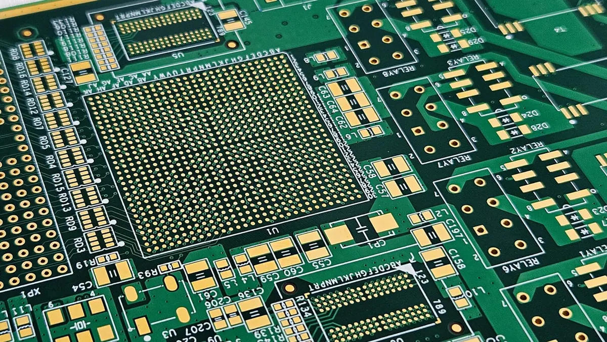
Direct Answer
Via-in-pad BGA PCB manufacturing should be planned around filled and capped vias, HDI stackup, pad geometry, solderability, X-ray inspection, and reflow risk before the design is released.
Engineering Context
Capability page for dense BGA routing where PCB fabrication and PCBA inspection decisions are tightly coupled.
Current taxonomy dimensions: pcbCategory: hdi, assemblyType: bga, layerCount: hdi-build-up.
Via In Pad BGA PCB is useful only when it changes the engineering or sourcing review. The page should make clear what the buyer must decide before quote, what the manufacturer can verify from the supplied package, and which assumptions would create rework if they are discovered after fabrication or assembly starts.
The key decision is: Plan via-in-pad BGA PCB manufacturing and assembly with filled-via, X-ray, and yield risks visible. A good RFQ connects that decision to concrete constraints, required handoff files, inspection scope, sourcing boundaries, and test evidence. If a requirement changes stackup, BOM control, fixture access, inspection depth, or shipment documentation, it belongs in the quote package rather than in a late email thread.
The relevant dimensions are pcbCategory: hdi, assemblyType: bga, layerCount: hdi-build-up. Each dimension should affect the quote inputs, manufacturing risks, or quality checks. A material, platform, industry, or capability label is not enough by itself unless it changes the actual review path.
Source-Backed Review Notes
- IPC official resources define the standards boundary for PCB design and workmanship without reproducing paid text.
- TI high-speed layout guidance supports early via, pad, return-path, and BGA escape review for dense boards.
- Existing OminiPCB content supplies via-in-pad and BGA assembly context.
Manufacturing Constraints
- voiding or solder wicking when via treatment is wrong
- extra lamination or filling process cost
- BGA rework difficulty after assembly
- yield loss when HDI stackup is not reviewed early
Quote Inputs
- BGA package data and pitch
- via structure and fill/cap requirements
- HDI buildup and layer count
- surface finish and solder mask notes
- X-ray inspection scope and acceptance criteria
Example Review
A compact processor module with a 0.5 mm pitch BGA should be quoted with BGA package data, escape-routing plan, HDI buildup, via fill and cap notes, surface finish, X-ray expectations, and rework assumptions. If the RFQ only says BGA PCB, the supplier cannot estimate the process risk accurately.
Pre-Quote Review
Before requesting Via In Pad BGA PCB, compare the design against adjacent options in the same cluster. If another material, platform, finish, or assembly route would use the same quote inputs and risk controls, the project may not need a separate sourcing path.
Source-backed notes should be used as engineering boundaries, not as copied datasheet text, standards excerpts, legal advice, or unsupported certification claims. The RFQ should describe the real product, operating environment, files, and acceptance checks that the manufacturer can verify.
The final quote package should make responsibility clear: design intent and acceptance criteria come from the buyer; DFM, fabrication, assembly, inspection, sourcing feedback, and delivery feasibility come from the manufacturing review.
Tradeoffs
- Via-in-pad can unlock dense BGA routing but adds fabrication process steps.
- Filled and capped vias reduce solder wicking risk but increase cost and review burden.
- Capability pages should show distinct manufacturing value through process steps, inspection scope, cost drivers, and failure modes.
CTA
Request a PCB quote when Gerber, stackup, BOM, quantity, lead time, and inspection requirements are ready for review.