
Direct Answer
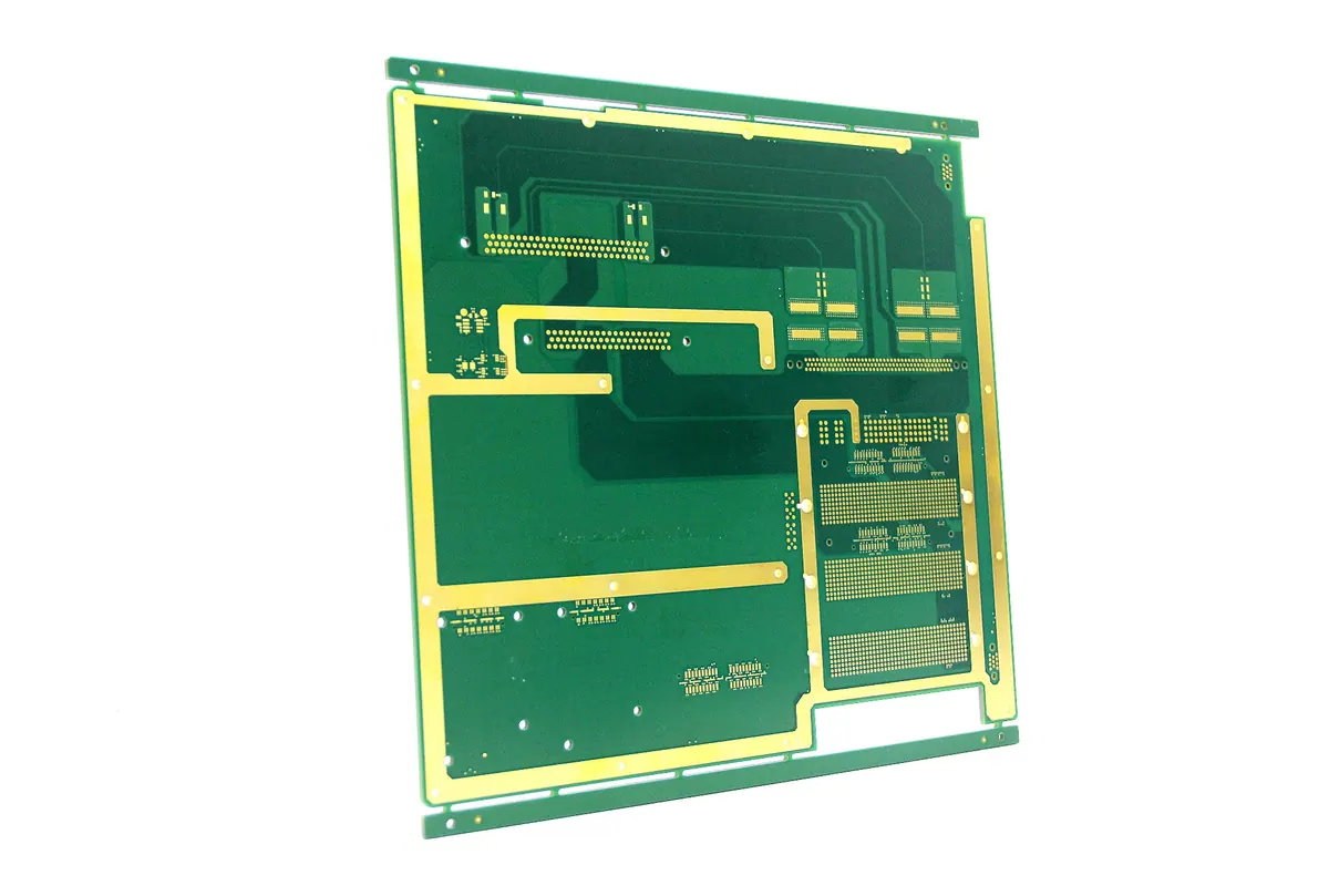
Heavy copper PCBs are specialized circuit boards designed to handle high electrical currents and manage heat effectively. They feature copper layers weighing 3 oz/ft² or more, significantly thicker than the standard 1 oz found in most FR4 PCBs. This added copper mass allows them to carry higher currents without excessive temperature rise, making them essential in power electronics, automotive systems, and industrial equipment where reliability under load is critical.
These boards are not simply thicker versions of standard PCBs; their fabrication demands precise process control to avoid defects like over-etching, delamination, or uneven plating. Manufacturers like Omini apply tailored DFM checks and process adjustments to ensure structural integrity and electrical performance in heavy copper designs.
Construction and Fabrication Process
The construction of a heavy copper PCB begins with selecting a suitable substrate, typically FR4 or a high-Tg variant, laminated with copper foil of 3 oz/ft² or greater. In multilayer builds, heavy copper layers may be used exclusively for power planes or high-current paths, while inner signal layers use standard 1 oz copper for finer routing.
Fabrication diverges from standard PCB processes during etching and plating. Because thick copper resists uniform chemical attack, etching times must be extended and carefully monitored to avoid undercutting or uneven sidewalls. Plating processes, especially for through-holes and vias, require higher current densities and longer durations to achieve full copper deposition thickness the tip. To mitigate these challenges, manufacturers often use techniques like differential etching or step plating.
Drilling and surface finish application also need adjustment. Thicker copper can increase tool wear during drilling, necessitating optimized parameters to prevent burring or delamination. Surface finishes such as HASL, ENIG, or OSP are applied after etching, but adhesion must be verified since thick copper surfaces can affect wetting and bonding.
Key Properties and Performance Advantages
The primary advantage of heavy copper is its ability to carry high current with minimal voltage drop. For example, a 100-mil wide trace using 2 oz copper can safely carry around 2–3 amps, while the same width with 6 oz copper can handle 6–8 amps or more, depending on temperature rise limits. This reduces the need for parallel traces or external busbars, simplifying layout and improving reliability.
Thermal performance is another key benefit. Copper’s high thermal conductivity allows heat to spread quickly from power components across the board, reducing hotspots. When combined with thermal vias or copper inlays, heavy copper layers act as effective heat spreaders, improving overall system thermal management.
Mechanically, heavy copper adds rigidity and resistance to thermal cycling stress. This is particularly valuable in automotive and industrial environments where boards undergo repeated temperature swings. The increased mass also improves resistance to peel-off during reflow soldering, especially for high-power components like MOSFETs or IGBTs.
Applications in Power Electronics and Industrial Systems
Heavy copper PCBs are most commonly found in power conversion systems. In DC-DC converters and voltage regulators, they enable efficient power delivery to processors, FPGAs, and memory modules. In motor drives and inverters, thick copper traces connect IGBT modules to DC-link capacitors, minimizing inductance and resistive losses.
In the automotive sector, especially electric vehicles (EVs), heavy copper supports onboard chargers, DC-DC converters, and battery management systems (BMS). These systems require reliable current handling at 48V or higher, often with strict space and weight constraints.
Industrial applications include welding equipment, uninterruptible power supplies (UPS), and motor control centers where continuous high-current operation is expected. Renewable energy systems, such as solar inverters and wind turbine converters, also rely on heavy copper for efficient power conversion at scale.
Design Considerations and DFM Review
Designing with heavy copper requires early attention to trace width, spacing, and thermal management. Designers must use electro-thermal simulation tools to predict temperature rise under load, ensuring compliance with safety standards like IPC-2152. Trace spacing must also account for increased electric field concentration at sharp corners, which can elevate the risk of arcing in high-voltage designs.
Thermal vias are frequently used to transfer heat from power components to internal or external copper layers. In heavy copper designs, these vias may be filled or plated shut to enhance thermal conductivity while maintaining structural integrity.
A thorough DFM review is essential before fabrication. Manufacturers like Omini evaluate Gerber files for potential issues such as inadequate annular ring, insufficient clearance between heavy copper features, or plating risks in deep vias. Adjustments may include modifying trace geometry, adding reliefs, or adjusting layer stackup to balance electrical needs with manufacturability.
Comparison with Standard FR4 PCBs
While standard FR4 PCBs with 1 oz copper suffice for most low-power digital and analog circuits, they fall short in high-current scenarios. The production process for heavy copper PCBs differs significantly, particularly in etching control, plating thickness, and thermal stress management. For a detailed comparison, see our guide on Different Production Process Between Heavy Copper PCB and FR4 PCB.
Heavy copper also influences stackup decisions. Designers may opt for asymmetric builds where only specific layers use thick copper, reducing cost and weight while preserving performance where needed. This approach contrasts with uniform heavy copper boards, which are heavier and more expensive but offer maximum current capacity.
Related Manufacturing Insights
Understanding heavy copper design also benefits from familiarity with related topics. For example, double-sided boards are often used in simpler power applications, and their advantages are detailed in Double Sided PCB: Advantages, Applications, and Manufacturing Process.
In flexible circuits, thick copper can be used but requires careful bending radius calculations; learn more in Flex PCB Material: Construction, Classification, and Advantages.
Finally, ensuring quality in assembly is critical. After fabrication, heavy copper boards undergo SMT assembly where inspection methods like AOI and X-ray help detect voids, insufficient wetting, or tombstoning—details covered in AOI and X-Ray Inspection in PCB Assembly.
Practical Notes from the Floor
In production, we’ve seen heavy copper designs fail not from lack of copper thickness, but from overlooked details like sharp trace corners causing etching unevenness or missing thermal vias leading to localized overheating. Addressing these in DFM prevents costly reworks.
For teams starting a heavy copper project, begin with a clear current budget and thermal target. Use that to define copper weight and trace geometry, then involve your manufacturer early. Omini’s engineering team reviews Gerber and BOM files to flag risks like inadequate spacing or plating concerns before any copper is etched.
The goal isn’t just to make a board that works—it’s to make one that lasts. Heavy copper PCBs deliver that durability when designed and built with precision, turning high-current challenges into reliable, field-proven solutions.