
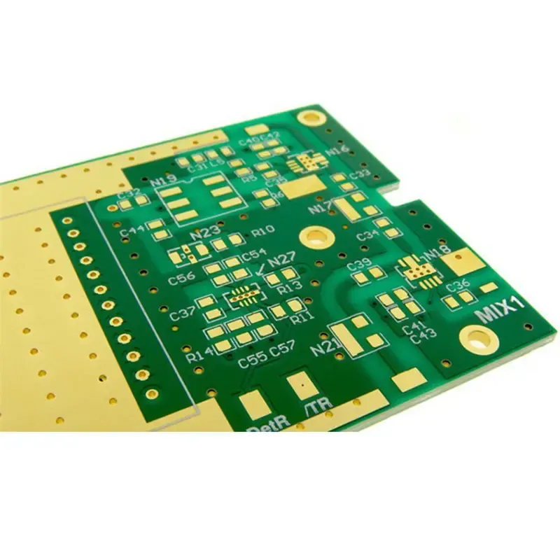
Direct Answer
High-speed PCBs are not defined by a specific frequency threshold but by the relationship between signal rise time and trace propagation delay. When rise times are fast enough that transmission line effects dominate, designers must treat traces as controlled impedance paths. This requires attention to dielectric materials, stackup symmetry, trace width/spacing, and via design to prevent signal reflection, crosstalk, and timing skew. Manufacturing must preserve these design intent through tight tolerances in etching, lamination, and drilling.
For Omini RFQs, translating high-speed design into production starts with DFM review of Gerber files, impedance-controlled layers, trace/space limits, stackup notes, and via aspect ratios. Material selection must align with the design's frequency requirements, and surface finish choices should be checked against solderability and signal-integrity needs.
PCB Stack-Up and Signal Integrity for High-Speed Boards
The foundation of any high-speed PCB is its stackup. Symmetric layer construction helps prevent warpage during lamination and ensures balanced electrical properties. Signal layers should be routed adjacent to solid ground or power planes to provide a low-inductance return path. For high-speed designs, microstrip and stripline configurations are preferred over buried signals without adjacent planes, as they offer predictable impedance and better shielding.
Dielectric thickness between signal and reference planes directly sets impedance; tighter tolerances on prepreg and core thickness are essential. Using a tool like the one discussed in our guide on PCB Stack-Up and Signal Integrity for High-Speed Boards helps simulate impedance before fabrication. During RFQ, stackup proposals should be checked against material datasheets and achievable impedance targets.
Decoding High-Density Interconnect (HDI) PCB Technology: An Overview
High-speed designs often drive the need for HDI technology, especially when routing BGAs or fine-pitch components. Microvias, blind vias, and buried vias reduce layer count and shorten signal paths, which is critical for maintaining signal integrity in high-frequency circuits. However, HDI introduces manufacturing complexity—laser drilling reliability, via filling, and plating uniformity become key yield factors.
In our overview of Decoding High-Density Interconnect (HDI) PCB Technology: An Overview, we cover how sequential lamination cycles affect dielectric stability and how via-in-pad designs require careful planarization to avoid solder joint defects. For high-speed applications, the RFQ should define via aspect ratio, fill material, and plating expectations so via structures do not introduce avoidable impedance discontinuities.
Decoding PCB: What PCB Board Stands For in Electronics
Understanding the basics helps contextualize high-speed challenges. As explained in Decoding PCB: What PCB Board Stands For in Electronics, a PCB provides mechanical support and electrical interconnection. In high-speed applications, the interconnection function becomes dominant—trace geometry, dielectric properties, and via design directly impact signal fidelity. A high-speed PCB must preserve the designer’s intended impedance, propagation delay, and mode conversion characteristics from schematic to physical board.
This means manufacturing processes like etching must maintain tight linewidth control—often ±10% or better for 50-ohm impedance traces. Lamination must avoid resin starvation or excess, which changes dielectric thickness. Drilling, especially for microvias in HDI stacks, must be clean and perpendicular to prevent via breakage or plating voids that disrupt high-frequency current flow.
Embedded PCB: A Comprehensive Guide for Beginners
Embedded components—such as resistors, capacitors, or inductors laminated within the PCB layers—can improve high-speed performance by shortening interconnections and reducing parasitic inductance. As detailed in Embedded PCB: A Comprehensive Guide for Beginners, embedding requires precise material compatibility and lamination control to avoid delamination or cracking.
For high-speed designs, embedded passives can minimize stub lengths and improve decoupling effectiveness near high-speed ICs. However, the embedding process adds thermal and mechanical stress during lamination. CTE matching between embedded components and laminate should be reviewed for temperature-cycling environments.
Circuit Board Manufacturing Process: A Comprehensive Guide for Beginners
The full manufacturing flow—from Gerber to finished board—must be optimized for high-speed fidelity. In our guide on Circuit Board Manufacturing Process: A Comprehensive Guide for Beginners, we walk through each step: imaging, etching, lamination, drilling, plating, solder mask, and surface finish.
For high-speed PCBs, critical control points include:
- Imaging: Minimum line width/space resolution to hit impedance targets
- Etching: Uniform copper removal to avoid trace width variation
- Lamination: Void-free bonding and thickness control of dielectrics
- Drilling: Laser via quality and mechanical drill accuracy for through-holes
- Plating: Uniform copper thickness in vias and on traces
- Surface finish: Consistent application for solderability and signal integrity
First-article inspection may include impedance testing by the method agreed for the order to validate that the manufactured board matches design intent before full production.
Material Selection and Loss Tangent
Dielectric loss tangent (Df) becomes significant above 1 GHz. Materials with low Df—such as PTFE-based laminates or reinforced hydrocarbon systems—reduce signal attenuation. However, these materials often have higher CTE or lower Tg, creating tradeoffs with thermal reliability and processability.
FR-4 can be usable for some moderate-speed designs, while low-loss alternatives may be required as frequency, rise-time, loss budget, or impedance tolerance becomes stricter. During DFM, material dielectric properties should be matched to the target impedance, trace geometry, assembly process, and operating environment.
Surface Finish and High-Speed Reliability
Surface finish affects both assembly yield and long-term signal integrity. ENIG provides excellent solderability and oxidation resistance, making it ideal for fine-pitch BGAs and high-reliability applications. However, nickel corrosion (black pad) can be a concern if not properly controlled. Immersion silver offers good conductivity but is prone to tarnish; immersion tin is cost-effective but can whisker.
For high-speed PCBs, finish uniformity matters because thickness variation can affect solderability and, in some geometries, signal behavior. The RFQ should define whether finish-thickness evidence, solderability checks, or reflow compatibility review is required.
DFM and Yield Optimization
DFM for high-speed PCBs goes beyond basic manufacturability checks. It includes impedance verification, skew analysis between differential pairs, and via stub impact assessment when those items are in scope. The review should also check acute angles, teardrops, and copper balancing to prevent etching inconsistencies that could cause impedance variation.
Yield is improved by designing with manufacturable tolerances—e.g., specifying 4-mil trace/space with a 2-mil allowance rather than pushing to 3-mil/3-mil. Panelization is optimized to minimize thermal stress during lamination, and fiducial placement is verified for accurate layer-to-layer registration, which is critical for microvia alignment in HDI stacks.
Practical Field Note
In production, the difference between a high-speed design that works and one that fails often comes down to tight control in etching, lamination, drilling, and plating. Visual inspection alone cannot prove high-speed performance, so critical programs should define impedance coupons, cross-section checks, X-ray scope, or functional validation before fabrication release. High-speed PCB success relies on close collaboration between design and manufacturing, where DFM is a continuous feedback loop rather than a late gate.