
Direct Answer
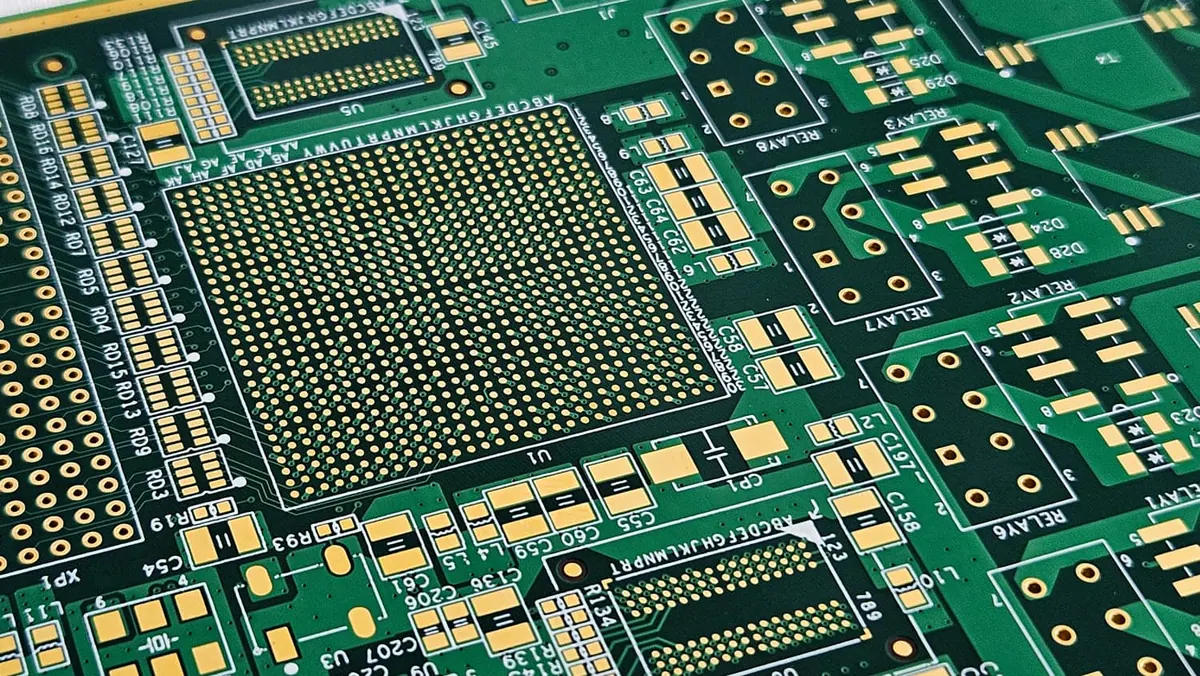
High-Density Interconnect (HDI) PCB technology represents a fundamental shift in how we route signals on a circuit board, moving away from simple through-hole drilling to a complex system of laser-drilled microvias and sequential lamination. Unlike standard PCBs where a single drill bit penetrates the entire board thickness, HDI allows vias to connect only specific layers, freeing up valuable real estate for routing traces and placing components. This capability is the backbone of modern miniaturization, enabling everything from compact wearables to high-performance computing modules.
However, the transition to HDI is not merely a design choice; it is a manufacturing constraint that demands strict adherence to specific fabrication protocols. The process involves building the board in stages, laminating copper and dielectric layers, drilling microvias with lasers, and repeating the cycle. This sequential build-up requires precise registration control and specialized surface finishes to handle fine-pitch components. For engineers, understanding the interplay between stackup design, via-in-pad requirements, and the limitations of laser drilling is the difference between a successful prototype and a costly production failure.
The Mechanics of Sequential Lamination and Microvias
The core of HDI technology is the sequential lamination process. In a standard multi-layer board, all layers are stacked, drilled, and plated in one massive operation. In contrast, an HDI board is built layer by layer. The process begins with a core, similar to a standard board, but then additional layers of prepreg and copper foil are laminated onto the surface. Once cured, a laser drill creates microvias that penetrate only the top dielectric layer to reach the underlying copper pad. After plating these microvias, the process repeats: more prepreg and copper are added, and the next set of microvias is drilled.
This method allows for the creation of blind vias (connecting an outer layer to one or more inner layers but not passing through the entire board) and buried vias (connecting inner layers without reaching the surface). The ability to place these vias directly under component pads, known as "via-in-pad," is a game-changer for routing density. It eliminates the need for long escape routes that consume board space, allowing for tighter component placement and smaller overall board footprints.
However, this complexity introduces significant manufacturing risks. The alignment tolerance for each lamination cycle is tight. If the registration drifts even slightly during the build-up, the microvia may miss its target pad, leading to an open circuit. This is why HDI fabrication requires advanced equipment and rigorous process control. At Omini, we see this challenge frequently when clients attempt to push the limits of trace width and spacing without accounting for the cumulative registration error of multiple lamination cycles. A design that looks perfect in simulation can fail in production if the aspect ratio of the microvia or the copper-to-dielectric ratio is not optimized for the specific fabrication house's capabilities.
Design for Manufacturing (DFM) Rules for HDI
Designing for HDI requires a mindset shift from "can it be routed?" to "can it be built?" The most critical DFM consideration is the aspect ratio of the microvias. While mechanical drills struggle with high aspect ratios, laser drills are limited by the depth they can penetrate relative to the via diameter. Typically, the aspect ratio for laser-drilled microvias should not exceed 1:1. If a via is too deep relative to its width, plating will be inconsistent, leading to voids or weak connections that fail reliability testing.
Another common pitfall is the handling of via-in-pad designs. While this technique maximizes routing density, it introduces thermal management challenges during the assembly process. If a via is filled with conductive epoxy and capped with copper, it provides a solid thermal path. However, if the via is not properly filled, solder can wick down into the hole during reflow, causing a "solder starvation" defect where the component pad lacks sufficient solder. This is particularly dangerous for Ball Grid Array (BGA) packages where every milligram of solder counts. Engineers must specify whether vias are tented, filled, or capped in the Gerber files and BOM to ensure the assembly team can apply the correct solder paste stencil design.
Furthermore, the choice of dielectric material becomes more critical in HDI. Standard FR-4 may not offer the dimensional stability required for multiple lamination cycles, leading to warpage or delamination. High-Tg (glass transition temperature) materials or specialized HDI laminates are often necessary to withstand the thermal stress of repeated heating and cooling. When preparing your design files, it is essential to run a thorough DFM check that specifically looks for these HDI-specific constraints. For a deeper dive into managing these constraints in complex geometries, reviewing Rigid-Flex PCB DFM Tips Before PCB Manufacturing can provide valuable context on how material selection and layer alignment interact in high-complexity builds.
Stackup Strategies and Signal Integrity
The stackup is the architectural blueprint of an HDI board, and getting it wrong can compromise both signal integrity and manufacturability. In high-speed designs, the placement of reference planes is non-negotiable. Every signal layer must have an adjacent reference plane (power or ground) to maintain a controlled impedance and minimize electromagnetic interference (EMI). In an HDI context, this often means that the microvia transitions must be designed to minimize stub length, which can cause signal reflections at high frequencies.
A common strategy for HDI stackups is the "any-layer" HDI approach, where vias can connect any two layers. While this offers maximum routing freedom, it significantly increases the cost and complexity of the stackup. A more balanced approach is the 1+N+1 or 2+N+2 stackup, where only the outer layers utilize microvias, and the inner core remains a standard multi-layer build. This hybrid approach often provides the best balance between performance and cost. However, the transition between the microvia layers and the core layers must be managed carefully to avoid impedance discontinuities.
Understanding the relationship between the stackup and signal behavior is vital. As trace widths shrink to accommodate higher density, the resistance of the traces increases, which can lead to signal attenuation. Additionally, the proximity of traces increases the risk of crosstalk. Engineers must perform rigorous simulation to ensure that the chosen stackup supports the required data rates. For a comprehensive analysis of how layer arrangement affects performance, refer to our detailed guide on PCB Stack-Up and Signal Integrity for High-Speed Boards. This resource breaks down the physics of return paths and how to optimize your stackup for both high-speed signaling and manufacturability.
Surface Finish and Assembly Considerations
Once the board is fabricated, the surface finish becomes the critical interface for component assembly. In HDI designs, the choice of surface finish is rarely optional; it is dictated by the pitch of the components. Hot Air Solder Leveling (HASL) is generally unsuitable for HDI boards with fine-pitch components (0.5mm pitch or less) because the process leaves an uneven surface. The air knives used to level the solder cannot effectively clear the solder from between tiny pads, leading to bridging and shorts.
Electroless Nickel Immersion Gold (ENIG) is the industry standard for HDI manufacturing. It provides a flat, planar surface that is ideal for fine-pitch placement. The nickel layer acts as a barrier, while the gold layer protects the nickel from oxidation. However, ENIG introduces its own set of challenges, such as the risk of "black pad" syndrome, where the nickel surface corrodes, leading to brittle solder joints. This risk is heightened in HDI boards where the via-in-pad structures are exposed to the surface finish process. To mitigate this, the plating chemistry must be tightly controlled, and the board design should avoid exposing large areas of bare copper that are difficult to plate uniformly.
Alternative finishes like Immersion Silver or Organic Solderability Preservative (OSP) exist but come with their own trade-offs regarding shelf life and handling. Immersion Silver offers good flatness but is prone to tarnishing, while OSP is cost-effective but has a short shelf life and is sensitive to handling. When selecting a finish, it is crucial to balance the assembly requirements with the long-term reliability needs of the product. For a detailed comparison of these options and their specific impact on yield, see ENIG vs OSP vs HASL for PCB Manufacturing. This comparison helps clarify why ENIG is often the default choice for high-density, high-reliability applications despite its higher cost.
Cost Drivers and Budget Management
One of the most common misconceptions in PCB manufacturing is that HDI is simply a more expensive version of a standard board. While it is true that HDI costs more, the cost drivers are specific and can be managed through smart design choices. The primary cost driver is the number of lamination cycles. Each additional cycle adds time, material, and labor. A 1+N+1 stackup is significantly cheaper than a 2+N+2 or 3+N+3 stackup. Therefore, optimizing the design to minimize the number of HDI layers is the most effective way to control costs.
Another major cost factor is the yield rate. HDI processes are more sensitive to defects. A single misaligned microvia can render an entire panel scrap. This sensitivity means that the yield curve for HDI is steeper than for standard boards. To maintain profitability, manufacturers often charge a premium for HDI to account for this risk. However, this premium can be mitigated by adhering to strict DFM rules and avoiding "over-engineering" the design. For instance, using the smallest possible via size or the tightest trace spacing without a functional need adds unnecessary risk and cost.
It is also important to consider the total cost of ownership, not just the unit price. A cheaper HDI board that fails in the field due to a manufacturing defect will cost far more in returns and reputation damage than a slightly more expensive, high-quality board. Avoiding the pitfalls of cutting corners is essential. Many teams fall into the trap of Cheap PCB Manufacturing: Common Mistakes That Kill Your Budget by selecting a vendor based solely on price without verifying their HDI capabilities. This often results in delayed timelines and compromised quality. Investing in a partner with proven HDI experience and robust quality control systems is a strategic decision that pays off in reliability and reduced total cost.
Final Field Notes on HDI Implementation
Implementing HDI technology is a journey that requires collaboration between design engineers and manufacturing partners. It is not enough to simply specify "HDI" in the design file; the intent must be communicated clearly through the stackup definition, Gerber files, and assembly drawings. The complexity of the process means that early engagement with the manufacturer is crucial. A pre-production review of the Gerber data can identify potential issues with via placement, aspect ratios, and impedance control before any material is cut.
As the industry moves toward smaller form factors and higher performance, HDI will continue to be the standard for advanced electronics. However, the margin for error is slim. Success depends on a deep understanding of the fabrication process, a commitment to rigorous DFM, and a partnership with a manufacturer who understands the nuances of sequential lamination and microvia plating. Whether you are building a wearable medical device or a high-speed communication module, the principles of HDI remain the same: precision, planning, and process control are the keys to unlocking the full potential of high-density design.