
Direct Answer
Chasing the lowest PCB fabrication quote almost always costs more. The real expense hides in rework, delayed prototypes, failed first-article inspections, and products that fail in the field. The most common mistake is treating PCB manufacturing as a commodity purchase rather than a design-for-manufacturing partnership. Engineers who optimize for unit price at the expense of DFM compliance, complete data packages, and appropriate material selection consistently see their total program cost climb by 20–40%.
Mistake 1: Submitting Incomplete Gerber and Fabrication Data
A surprising number of RFQs arrive with missing solder mask layers, incomplete drill files, or no fabrication notes at all. Cheap PCB manufacturing quotes are generated by automated systems that parse your data package. When critical layers are absent, the quote engine either rejects the job or applies conservative assumptions that inflate price.
Missing impedance control notes are particularly expensive. A fabricator cannot guess whether your 50 Ω traces are calculated for microstrip or stripline, or which dielectric constants to apply. Without explicit stackup requirements, they default to standard constructions that may not meet your signal integrity needs. You then face a choice: accept compromised performance or pay rush fees to re-spin.
Before submitting, verify your Gerber output against IPC-D-356 netlist data. Include a detailed fabrication drawing with board dimensions, hole tolerances, surface finish specification, and any special requirements like edge plating or controlled depth drilling. This discipline prevents the back-and-forth that cheap quotes assume away.
Mistake 2: Ignoring DFM Until After Fabrication Begins
Design for manufacturability is not a post-layout checkbox. It is a continuous discipline that starts during schematic capture and constrains every placement and routing decision. Teams that skip formal DFM review before releasing to PCB manufacturing capabilities frequently discover that their 3 mil trace-and-space rules, blind vias, or buried passives push the board into premium pricing tiers.
Common DFM oversights include insufficient annular ring, acid traps in copper pours, and non-standard aspect ratios in plated through-holes. These issues do not always cause immediate failure. Instead, they reduce process margin. When the fab house runs your board on a slightly worn drill bit or with chemistry near control limits, marginal designs fail while robust designs pass.
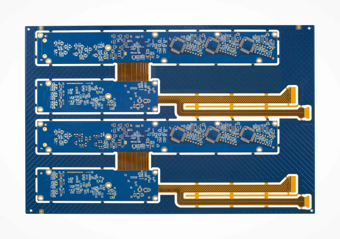
For rigid-flex designs, the consequences are more severe. Bend radius violations, improper coverlay openings, and stiffener placement errors cannot be patched. They require full re-fabrication. Review Rigid-Flex PCB DFM Tips Before PCB Manufacturing early in your mechanical design phase to avoid these traps.
Mistake 3: Selecting Surface Finish Based on Price Alone
HASL, ENIG, OSP, and immersion tin each carry different material costs, but the cheapest option rarely minimizes total cost of ownership. HASL's uneven surface creates coplanarity problems for fine-pitch QFNs and BGAs. ENIG offers flatness and shelf life but introduces black pad risk if plating chemistry drifts. OSP is economical and solderable but degrades with multiple thermal cycles and long storage.
Your assembly process, component package types, and product shelf life should drive finish selection, not the fabrication line item. High-reliability products with long field lives and storage periods before assembly typically justify ENIG despite higher upfront cost. Consumer products with rapid assembly turnaround and cost pressure may tolerate OSP with careful inventory management.
Compare the tradeoffs systematically. ENIG vs OSP vs HASL for PCB Manufacturing provides a framework for matching finish to your specific reliability and assembly requirements.
Mistake 4: Mismatched Stackup and Material Selection
Stackup design sits at the intersection of electrical performance, thermal management, and fabrication cost. Engineers sometimes specify exotic low-Dk laminates for modest speed requirements, or conversely attempt to route high-speed signals through standard FR-4 with inadequate layer count. Both errors are expensive.
The first inflates material cost without commensurate benefit. The second creates signal integrity failures that manifest as intermittent bit errors, hard debug time, and eventual layer addition in a re-spin. Neither is necessary with proper upfront analysis.
Work with your fabricator to validate stackup before finalizing placement. PCB Stack-Up and Signal Integrity for High-Speed Boards explains how dielectric thickness, copper weight, and prepreg selection interact to determine impedance and crosstalk. Omini's engineering team reviews customer stackups against both electrical targets and our PCB manufacturing capabilities to flag mismatches before they become change orders.
Mistake 5: Underspecifying or Overspecifying Tolerances
Tight tolerances are not free. A ±5% impedance specification requires more precise etching, more frequent cross-sections, and higher scrap rates than ±10%. Similarly, demanding ±0.05 mm drilled hole positional tolerance when your design only needs ±0.1 mm adds inspection burden with no functional benefit.
Conversely, loose tolerances in critical areas create assembly headaches. Insufficient soldermask clearance around fine-pitch pads leads to solder bridging. Inadequate keepout around mounting holes causes shorts to chassis ground. The discipline is tolerancing each feature to its functional requirement, not uniformly tightening or relaxing everything.
Review your design against IPC-6012 class requirements. Class 2 covers most commercial applications. Class 3 adds cost for medical, military, and other high-reliability applications where failure has severe consequences. Specifying Class 3 for a consumer wearable is waste. Specifying Class 2 for a pacemaker is negligence.
Mistake 6: Neglecting the Assembly Interface
PCB fabrication decisions directly impact PCB assembly capabilities. Panelization strategy, fiducial placement, and component keepout zones all originate in layout but determine SMT throughput and yield. A panel array that maximizes board count per panel may minimize fab cost while destroying assembly efficiency if it forces manual handling or non-standard fixture investment.
Component proximity to board edges affects depanelization stress and potential solder joint cracking. Fiducial design and placement determine vision system registration accuracy. Omitting these considerations in pursuit of cheaper bare boards externalizes cost to the assembly house, who passes it back through higher assembly quotes or rejects marginal product.
For turnkey programs, BOM Risk Strategy for Turnkey PCB Assembly becomes equally important. A cheap PCB with an unprocurable BOM is inventory, not product. Omini's EMS service model integrates component sourcing intelligence with fabrication planning to avoid these dead ends.
Mistake 7: Skipping First Article and Process Validation
The final and most expensive mistake is assuming that a passing electrical test at the fabricator guarantees good product. Fabrication electrical test verifies continuity and isolation, not long-term reliability, solder joint quality, or performance under environmental stress.
First article inspection should include dimensional verification, microsection analysis for plating thickness and via quality, and thermal cycling if the product sees temperature extremes. For high-reliability applications, AOI and X-Ray Inspection in PCB Assembly extends validation into the assembly process, catching voids in thermal pads, insufficient fill in QFN ground connections, and other defects invisible to electrical test alone.
Skipping these steps accelerates initial delivery but defers discovery to field failure, where remediation costs multiply by orders of magnitude. The cheapest PCB is the one that works the first time, every time, for the product's entire life.
Building Cost Discipline Without False Economy
Cheap PCB manufacturing is achievable, but it requires understanding where costs actually originate. Incomplete data, ignored DFM, inappropriate material choices, and poor assembly interface design each create hidden expenses that dwarf any fabrication quote savings. The engineers who manage total cost treat the fabricator as a partner whose expertise they leverage early, not a vendor they squeeze late.
Omini supports this approach by integrating fabrication, assembly, and supply chain planning under one program management structure. When your PCB manufacturing capabilities conversation happens alongside assembly process review and component availability analysis, the expensive surprises disappear. That is the only kind of cheap worth pursuing.