
Direct Answer
PCB stands for Printed Circuit Board. It is the physical platform that mechanically supports and electrically connects electronic components using conductive tracks, pads, and other features etched from one or more sheet layers of copper laminated onto a non-conductive substrate. The term "PCB board" is widely used in the industry, though technically redundant, as it emphasizes the physical nature of the component against the schematic design. In a manufacturing context, a PCB is the result of a complex fabrication process involving photolithography, etching, drilling, and plating to create the interconnects that allow current to flow between resistors, capacitors, ICs, and connectors.
The journey from a digital schematic to a physical PCB involves strict adherence to design rules that dictate trace width, spacing, and via placement. At Omini, we see that the most common failures in early production runs stem not from the circuit logic itself, but from overlooking the physical constraints of the fabrication process. Whether it is a simple two-layer board for a consumer gadget or a complex high-reliability PCB for medical equipment, the fundamental definition remains the same: it is the backbone of the electronic assembly. Understanding what PCB stands for is the first step, but mastering the nuances of fabrication, from the copper weight to the surface finish, is what separates a functional prototype from a mass-producible product.
The Fabrication Reality: From Gerber to Finished Board
When engineers discuss PCB manufacturing, they are often referring to the intricate dance between digital design files and chemical processing. The process begins with the Gerber files, which act as the blueprint for the fabrication house. These files define the copper layers, solder mask, silkscreen, and drill data. However, a Gerber file is only as good as the design rules applied to it. A common pitfall is assuming that a design that looks correct in the CAD tool will automatically translate to a manufacturable board. This is where Design for Manufacturability (DFM) becomes the gatekeeper of success.
In a typical fabrication workflow, the inner layers are first patterned using photoresist and etched to form the circuit traces. These layers are then laminated together with prepreg (a fiberglass material impregnated with resin) and core material under high heat and pressure. The stackup design is critical here; it determines the electrical performance, impedance control, and thermal management of the final product. For high-speed designs, the arrangement of signal and reference planes is non-negotiable. Engineers must carefully consider the dielectric constant of the materials and the distance between layers to maintain signal integrity. For a deeper dive into how layer arrangement affects performance, reviewing the principles of PCB Stack-Up and Signal Integrity for High-Speed Boards is essential for anyone designing complex systems.
Once the lamination is complete, the board is drilled to create holes for vias and through-hole components. The drilling process must be precise; even a slight deviation can lead to broken connections or short circuits. After drilling, the holes are plated with copper to establish electrical connections between the layers. This electroplating process is delicate, requiring strict control over current density and bath chemistry to ensure uniform copper thickness. If the plating is too thin, the board may fail reliability testing due to thermal cycling. If it is too thick, it can cause issues with hole fill and solderability.
The outer layers are then patterned and etched, leaving the final copper traces exposed. At this stage, the board undergoes a solder mask application, which is the green (or other colored) coating that insulates the copper traces and prevents solder bridges during assembly. The solder mask must be applied with precision to ensure that pads are exposed exactly where needed. Finally, the silkscreen is printed to add component designators and logos. The choice of surface finish at this stage is pivotal. It protects the exposed copper pads from oxidation and ensures a reliable solder joint during the assembly phase. The selection between ENIG, OSP, and HASL involves trade-offs between cost, shelf life, and solderability, as detailed in our analysis of ENIG vs OSP vs HASL for PCB Manufacturing.
Advanced Prototyping and High-Reliability Requirements
Not all PCBs are created equal. While a standard two-layer board might suffice for a simple LED controller, modern electronics often demand advanced technologies like high-density interconnect (HDI) or rigid-flex constructions. HDI technology allows for finer trace widths and smaller vias, enabling higher component density and better performance in compact devices. This is achieved through the use of microvias, which are laser-drilled holes that connect specific layers without penetrating the entire board. The complexity of HDI fabrication requires specialized equipment and a higher level of process control.
When exploring Decoding High-Density Interconnect (HDI) PCB Technology: An Overview, it becomes clear that the shift from through-hole vias to microvias changes the entire fabrication workflow. Laser drilling is slower and more expensive than mechanical drilling, but it allows for a much higher routing density. For products like smartphones, wearables, and advanced medical sensors, HDI is often the only viable option. However, the cost implications are significant, and the yield rates can be lower if the design rules are not strictly followed.
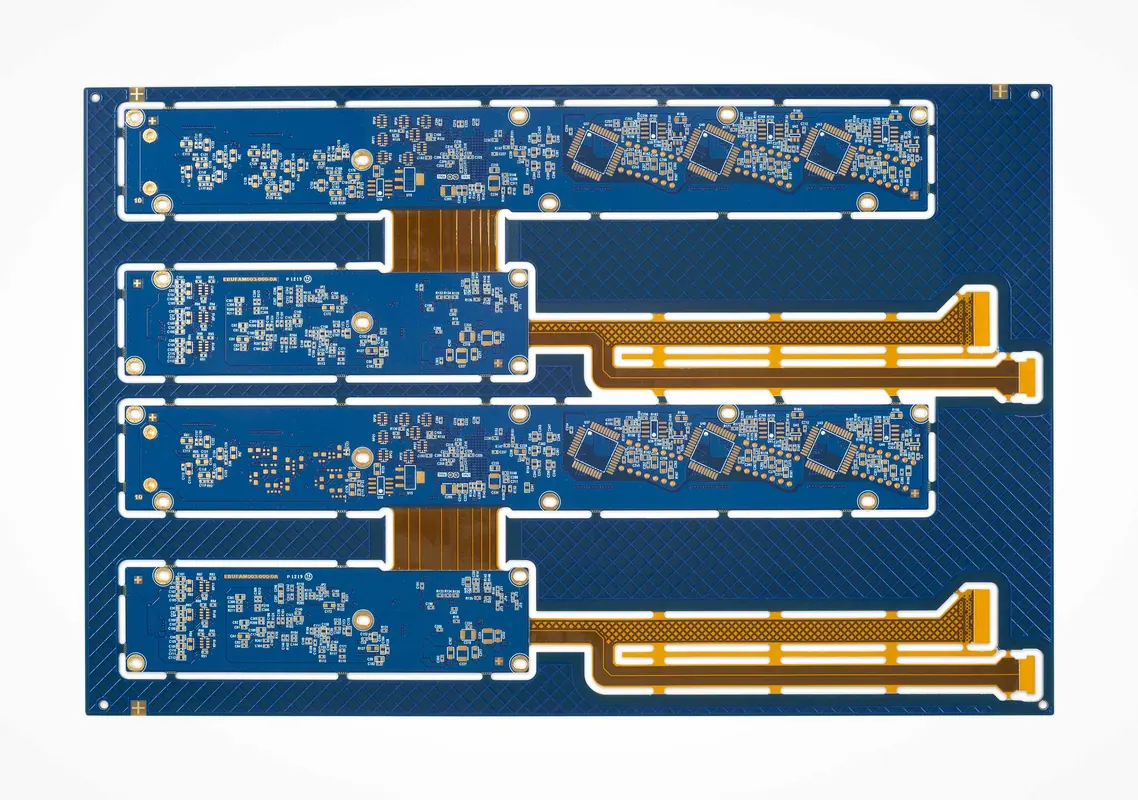
Rigid-flex PCBs represent another frontier in manufacturing complexity. These boards combine rigid sections, which provide structural support and mounting for heavy components, with flexible sections that can bend and fold. This hybrid approach eliminates the need for connectors and cables, reducing the overall weight and improving reliability in applications subject to vibration or movement. However, the fabrication of rigid-flex boards is notoriously difficult. The materials used for the flexible sections, such as polyimide, have different thermal expansion coefficients than the rigid FR-4 sections. If the stackup is not designed correctly, the board can delaminate or crack during thermal cycling.
To mitigate these risks, a rigorous DFM process is required before any material is cut. Engineers must account for the bending radius, the placement of copper traces in the flexible areas, and the reinforcement of the rigid sections. Rigid-Flex PCB DFM Tips Before PCB Manufacturing provides a comprehensive look at the specific design rules that prevent failure in these complex assemblies. At Omini, we often work with clients to refine their stackup designs to ensure that the transition between rigid and flexible sections is smooth and reliable. This proactive approach saves time and money by preventing costly re-spins.
High-reliability PCBs are another category that demands special attention. Used in aerospace, automotive, and medical applications, these boards must withstand extreme temperatures, vibration, and humidity. The materials selected for these boards, such as high-Tg FR-4 or specialized ceramics, are chosen for their thermal and mechanical properties. The fabrication process for high-reliability boards often includes additional testing steps, such as cross-sectioning to verify plating quality and automated optical inspection (AOI) to detect microscopic defects. The goal is to achieve a near-zero defect rate, which requires a manufacturing partner with deep expertise and robust quality control systems.
The Intersection of PCB Fabrication and PCBA Assembly
The journey of a PCB does not end at the fabrication house. Once the bare board is produced, it moves to the assembly stage, where components are placed and soldered. This transition is where the theoretical design meets the physical reality of component availability and assembly constraints. The quality of the PCB fabrication directly impacts the success of the assembly. For instance, if the solder mask is too thick or the pads are not properly defined, components may not solder correctly, leading to open circuits or cold joints.
Component sourcing is a major challenge in the current electronics landscape. Global supply chain disruptions have made it difficult to secure certain chips and passive components. A robust BOM strategy is essential to navigate these challenges. This involves identifying alternative parts, managing lead times, and ensuring that the design can accommodate substitutions without compromising performance. BOM Risk Strategy for Turnkey PCB Assembly outlines how to build a resilient supply chain that can adapt to market volatility. By working with an EMS provider who has a global network of suppliers, manufacturers can mitigate the risk of production delays.
The assembly process itself is a highly automated operation. Surface Mount Technology (SMT) machines place components onto the board with incredible speed and precision. The solder paste is applied using a stencil, and the components are placed using pick-and-place machines. The board then passes through a reflow oven, where the solder paste melts and forms the electrical connections. The temperature profile of the reflow oven must be carefully controlled to ensure that the solder melts properly without damaging the components or the PCB. Through-hole components are typically inserted and soldered using wave soldering or selective soldering processes.
Inspection is a critical part of the assembly process. Automated Optical Inspection (AOI) and X-ray inspection are used to detect defects such as missing components, misalignment, or solder bridges. For high-reliability applications, X-ray inspection is particularly important for checking the quality of solder joints in Ball Grid Array (BGA) packages, which are hidden beneath the component. If defects are found, the board is sent for rework. However, rework is costly and can weaken the board, so the goal is to get it right the first time. This requires close collaboration between the design team, the fabrication house, and the assembly partner.
Practical Considerations for Modern Electronics Design
Designing a PCB today requires a holistic view that spans from the initial concept to the final product launch. It is not enough to simply draw the schematic; engineers must consider the manufacturability, the supply chain, and the end-use environment. The choice of materials, the stackup design, and the surface finish are all decisions that have long-term implications for the product's performance and cost. A design that is easy to prototype but difficult to manufacture will face significant hurdles when scaling to mass production.
One of the most common mistakes is ignoring the tolerances of the fabrication process. Every manufacturer has limits on the minimum trace width, the smallest drill size, and the tightest spacing they can achieve. Designing to the absolute limit of these capabilities leaves no room for error and can lead to yield issues. It is often better to design with a margin of safety to ensure consistent quality. Additionally, the choice of components must be made with availability in mind. Using obsolete or hard-to-find parts can derail a project, even if the PCB design is perfect.
Collaboration with a knowledgeable manufacturing partner is invaluable. At Omini, we work with clients to review their designs before they go to production, identifying potential issues and suggesting improvements. This collaborative approach ensures that the final product is not only functional but also reliable and cost-effective. Whether it is optimizing the stackup for signal integrity, selecting the right surface finish for the application, or developing a robust BOM strategy, the right partner can make a significant difference.
As the industry moves towards smaller, faster, and more complex devices, the demand for advanced PCB technologies will continue to grow. The ability to decode the complexities of PCB manufacturing and navigate the challenges of assembly is a critical skill for any electronics engineer. By understanding the fundamentals and staying informed about the latest trends and technologies, designers can create products that stand the test of time. The path from a simple idea to a finished electronic device is paved with careful planning, precise execution, and a deep understanding of the manufacturing process. It is a journey that requires attention to detail and a commitment to quality at every step. The final product is a testament to the intricate balance between design innovation and manufacturing reality, where every trace, via, and component plays a vital role in the success of the whole.