
Direct Answer
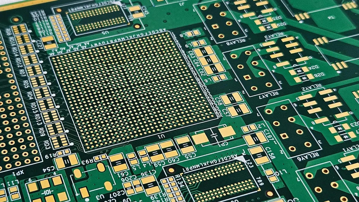
Double sided PCBs represent the industry standard for mid-complexity electronics, bridging the gap between the simplicity of single-sided boards and the high cost of multilayer designs. By utilizing copper traces on both the top and bottom surfaces connected via plated-through holes (vias), these boards allow for significantly higher component density and more efficient routing without the need for internal signal layers. The manufacturing process involves a critical electroplating step to ensure electrical continuity between layers, making design for manufacturability (DFM) essential to prevent common failures like via barrel cracks or annular ring violations.
From a production standpoint, the shift to double sided architecture often eliminates the need for jumper wires and reduces the overall board size, directly impacting the bill of materials and assembly costs. However, this complexity introduces specific challenges in drilling accuracy and plating quality that must be managed during fabrication. Understanding the nuances of via types, copper weights, and surface finishes is crucial for engineers aiming to balance performance with cost efficiency in their next project.
Understanding the Architecture and Electrical Advantages
The fundamental advantage of a double sided PCB lies in its ability to double the available routing area compared to a single-sided board. In a single-sided design, the component side is often reserved exclusively for parts, forcing all routing to occur on the solder side. This constraint frequently leads to complex jumper wire usage or larger board footprints to accommodate trace routing. With a double sided configuration, designers can place components on both sides of the board, although this is less common in high-density SMT assemblies due to reflow oven constraints. More typically, the bottom layer is utilized for ground planes or power distribution, while the top layer handles signal routing.
This architectural flexibility allows for better signal integrity management. Engineers can dedicate one layer to a solid ground plane, which provides a return path for signals and reduces electromagnetic interference (EMI). This is particularly important in mixed-signal designs where analog and digital circuits coexist. The ability to route traces on both sides also reduces the number of vias required for complex nets, as traces can cross over each other by simply moving to the opposite layer at a via point. This reduction in via count can improve yield rates and reduce the risk of open circuits during the plating process.
However, the transition to double sided designs requires careful consideration of the via structure. Unlike multilayer boards where blind or buried vias can be used to connect specific layers, double sided PCBs primarily rely on through-hole vias that penetrate the entire substrate. This means every via connects the top and bottom layers, which can sometimes lead to unnecessary copper exposure on layers that don't need it. Despite this, the cost-effectiveness of through-hole vias makes double sided PCBs the preferred choice for a vast range of applications, from consumer electronics to industrial control systems.
When evaluating the stackup for a double sided PCB, the core material selection becomes a primary factor in performance. Standard FR4 is sufficient for most applications, but high-frequency or high-temperature environments may require specialized materials like Rogers or high-Tg FR4. The dielectric constant and loss tangent of the material will influence signal propagation speed and attenuation. For designs requiring high reliability, the choice of prepreg and core thickness must align with the expected thermal cycling conditions to prevent delamination.
The Manufacturing Process: From Drilling to Plating
The fabrication of a double sided PCB introduces several critical steps that are absent in single-sided production, with drilling and electroplating being the most significant. The process begins with the preparation of the copper-clad laminate, where the base material is cleaned and etched to form the initial circuit pattern on both sides. Once the outer layer patterns are defined, the board undergoes a drilling operation to create holes for vias and component leads. The precision of this drilling step is paramount; the hole diameter must be consistent to ensure proper plating thickness and mechanical strength.
Following drilling, the board enters the electroplating stage, where a thin layer of copper is deposited onto the hole walls to create electrical connectivity between the top and bottom layers. This is the most critical quality control point in double sided manufacturing. If the plating is too thin, the via may crack under thermal stress, leading to an open circuit. If the plating is too thick, it can cause issues with hole fill or interfere with component insertion. The plating process also involves a chemical etching step to remove excess copper from the surface, leaving only the desired circuit traces.
After the copper plating is complete, the board undergoes a solder mask application to protect the copper traces from oxidation and prevent solder bridges during assembly. The solder mask is applied to both sides of the board, with openings left only where soldering is required. This step also serves to define the mechanical boundaries of the board and can include silkscreen printing for component identification and polarity markers. The final step in fabrication is the surface finish application, which protects the exposed copper pads and ensures good solderability.
The choice of surface finish is a critical decision that impacts both the manufacturing process and the long-term reliability of the assembly. Common options include Hot Air Solder Leveling (HASL), Electroless Nickel Immersion Gold (ENIG), and Organic Solderability Preservatives (OSP). Each finish has distinct advantages and trade-offs regarding shelf life, solderability, and cost. For detailed comparisons of these finishes and their suitability for different applications, refer to our analysis on ENIG vs OSP vs HASL for PCB Manufacturing. The surface finish must be compatible with the assembly process; for instance, ENIG is often preferred for fine-pitch components due to its flat surface, while HASL may be more cost-effective for through-hole components.
In high-volume production, the consistency of the plating process is monitored through statistical process control (SPC) to ensure that every board meets the specified copper thickness and hole quality standards. Any deviation in the plating bath chemistry or current density can result in non-uniform copper deposition, leading to yield losses. Manufacturers like Omini utilize advanced monitoring systems to maintain these parameters within tight tolerances, ensuring that the final product meets the rigorous demands of modern electronics.
Design for Manufacturability and Common Pitfalls
Designing a double sided PCB requires a deep understanding of the manufacturing constraints to avoid costly redesigns and production delays. One of the most common pitfalls is the violation of annular ring requirements. The annular ring is the amount of copper surrounding a via hole on a pad. If the ring is too small, drilling tolerances can cause the hole to break out of the pad, resulting in an open circuit. Designers must adhere to the manufacturer's minimum annular ring specifications, which typically range from 0.05mm to 0.1mm depending on the technology level.
Another critical consideration is the copper-to-edge clearance. Traces and pads must maintain a safe distance from the board edge to prevent damage during the panelization and depanelization processes. Insufficient clearance can lead to copper exposure on the edge of the board, causing short circuits or mechanical weakness. Additionally, the placement of vias near the edge of the board can be problematic, as the drilling process may cause micro-cracks in the substrate if the hole is too close to the edge.
Thermal management is also a significant concern in double sided designs, especially when components are placed on both sides. Heat dissipation can be less efficient compared to single-sided boards where the entire bottom layer can act as a heat sink. Designers should consider using thermal vias to transfer heat from the component side to the opposite layer or to an internal ground plane if available. However, in double sided boards, the bottom layer is often used for routing, which can limit the effectiveness of thermal vias. In such cases, increasing the copper weight or using a dedicated thermal pad can help mitigate overheating issues.
For more complex designs that push the boundaries of standard double sided capabilities, such as those requiring flexible sections or extreme durability, engineers often look toward rigid-flex solutions. Before finalizing a design that involves mixed rigid and flexible sections, it is crucial to review Rigid-Flex PCB DFM Tips Before PCB Manufacturing to understand the specific constraints and advantages of these hybrid structures. While double sided boards are robust, they lack the mechanical flexibility of rigid-flex designs, which can be a deciding factor in wearable or aerospace applications.
Furthermore, the density of components and the complexity of the routing can sometimes necessitate a transition to a different manufacturing process. For instance, if a design requires heavy copper traces to handle high currents, the standard double sided process may not be sufficient. In such scenarios, understanding the Different Production Process Between Heavy Copper PCB and FR4 PCB is essential. Heavy copper PCBs require specialized etching and plating techniques to accommodate the thicker copper layers, which can impact lead times and costs.
Applications and Selection Criteria for Manufacturers
Double sided PCBs are ubiquitous in the electronics industry, finding applications in everything from simple consumer gadgets to complex industrial control systems. Their versatility makes them the go-to choice for products that require more functionality than a single-sided board can provide but do not justify the cost of a multilayer stackup. Common applications include power supplies, automotive control modules, and telecommunications equipment. In these sectors, the reliability of the via connections and the quality of the surface finish are critical for ensuring long-term performance in harsh environments.
When selecting a manufacturer for double sided PCBs, it is important to evaluate their capabilities in handling the specific requirements of your design. Factors such as minimum trace width, via size, and surface finish options should be reviewed against the manufacturer's standard capabilities. A manufacturer with a strong focus on PCB Manufacturing will have the necessary equipment and expertise to handle complex double sided designs with high yield rates. It is also beneficial to choose a partner who offers comprehensive DFM support, as early feedback can prevent costly errors during production.
The decision to outsource PCB fabrication to a specialized EMS provider or a dedicated PCB fabricator often depends on the volume and complexity of the project. For high-volume runs, a manufacturer with automated production lines and rigorous quality control systems is essential. For low-volume prototypes, flexibility and speed are often more important. Omini, for example, positions itself as a strategic partner for both prototyping and mass production, offering a seamless transition from design to assembly. When evaluating potential partners, consider their experience with your specific industry and their ability to provide Double Sided PCB Fabrication: How to Choose the Right Manufacturer guidance tailored to your project needs.
Quality assurance is another critical factor in the selection process. Double sided PCBs are subject to various failure modes, including via cracking, solder mask delamination, and surface finish oxidation. A reputable manufacturer will employ advanced inspection techniques, such as Automated Optical Inspection (AOI) and X-ray inspection, to detect these defects before the boards are shipped. Understanding the role of these inspection methods is vital for ensuring the reliability of your final product. For a deeper dive into how these technologies safeguard your assembly, read about AOI and X-Ray Inspection in PCB Assembly.
Ultimately, the success of a double sided PCB project hinges on the collaboration between the design team and the manufacturing partner. Clear communication of design intent, adherence to DFM guidelines, and a thorough understanding of the manufacturing process are key to delivering a high-quality product. By carefully considering the advantages, applications, and process constraints of double sided PCBs, engineers can make informed decisions that optimize performance, cost, and reliability for their specific applications.
As you move forward with your next project, remember that the nuances of double sided PCB manufacturing often lie in the details. From the precise control of copper plating thickness to the strategic placement of thermal vias, every decision impacts the final outcome. Whether you are designing a simple control board or a complex industrial module, the principles of robust design and careful manufacturing selection remain constant. The field of PCB fabrication continues to evolve, with new materials and processes emerging to meet the demands of modern electronics. Staying informed about these developments and maintaining a strong partnership with your manufacturing provider will ensure that your designs not only function correctly but also stand the test of time in the field.