
Direct Answer
Selecting the right pcb fabrication partner is not just about price per square inch; it is about aligning manufacturing capabilities with your design intent, reliability targets, and assembly flow. For pcb manufacturing projects ranging from quick-turn pcb prototype boards to high reliability pcb production, you need clear visibility into stackup construction, material grades, surface finish selection, and DFM feedback loops. A partner that treats Gerber review and BOM risk as part of the process—not an afterthought—will protect your yield and reduce hidden costs across the product lifecycle. Whether you are sourcing a simple double-sided board or evaluating rigid flex pcb options, the evaluation criteria should remain consistent: process control, documentation, and scalability.
Material and Stackup Decisions That Drive Reliability
The foundation of every reliable board starts with the pcb stackup. Your stackup defines dielectric thickness, copper weight, prepreg selection, and impedance control—factors that directly influence signal integrity and thermal performance. In high reliability pcb applications, such as aerospace, medical, or industrial control systems, material selection moves beyond standard FR-4 to high-Tg, low-loss, or halogen-free laminates that withstand thermal cycling and humidity. You should request a detailed stackup drawing from your pcb fabrication supplier before releasing Gerber files, because an incorrect layer pairing or mismatched dielectric constant can cause impedance drift and delamination under load.
Copper weight and plating distribution also matter. Heavy copper boards used in power electronics require different etching tolerances and via plating strategies than standard signal boards. If your design includes buried or blind vias, confirm that your manufacturer can maintain registration accuracy across multiple lamination cycles. For pcb prototyping, it is acceptable to use a simplified stackup to validate form and fit, but you must document any deviations from the production stackup so that electrical performance can be correlated later. When you transition from pcb prototype to volume pcb manufacturing, the stackup should be locked, and any change should trigger a new DFM review and first-article inspection.
Dielectric loss tangent and glass transition temperature become critical when boards operate at elevated temperatures or high frequencies. A high reliability pcb built for outdoor telecom infrastructure, for example, may require a material with Tg above 170°C and a dissipation factor below 0.015 to maintain signal integrity over years of thermal stress. Your manufacturer should provide material datasheets and lot traceability, not just generic FR-4 labels. In pcb manufacturing, traceability is not paperwork; it is the mechanism that allows root-cause analysis when a field failure occurs. Without it, you are guessing whether a delamination event came from a bad prepreg batch, an out-of-spec lamination cycle, or an incorrect copper foil supplier.
Surface Finish, Solderability, and Long-Term Performance
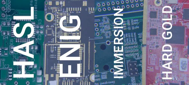
Surface finish selection is one of the most underestimated variables in pcb fabrication. The finish protects exposed copper, enables solder wetting during PCBA, and influences shelf life, contact resistance, and thermal cycling behavior. ENIG provides a flat, solderable surface ideal for fine-pitch BGA and long storage life, but it requires strict process control to avoid black pad defects. OSP is cost-effective and environmentally friendly, yet it offers limited shelf life and can degrade under multiple reflow cycles. HASL remains common for through-hole dominant designs but creates uneven surfaces that challenge fine-pitch SMT placement. For a deeper comparison of tradeoffs, review ENIG vs OSP vs HASL for PCB Manufacturing.
In high reliability pcb builds, surface finish must align with both assembly chemistry and end-use environment. If your product operates in high-humidity or corrosive conditions, ENIG or immersion silver may outperform OSP. If you are running a quick pcb prototyping cycle to validate a new design, OSP can reduce cost and lead time, provided you plan assembly within the recommended window. Always specify finish thickness, acceptance criteria, and storage conditions in your fabrication notes, because ambiguity here is a common source of solderability failures during turnkey PCBA.
Storage and handling conditions extend beyond the factory floor. Boards with OSP or immersion silver should be packaged in moisture-barrier bags with desiccant and humidity indicators, especially when shipping across climates. During pcb manufacturing, the finish line should be monitored for bath chemistry, temperature, and dwell time, with statistical process control charts available on request. If your partner cannot provide these records, you are relying on luck rather than process control. For rigid flex pcb designs, surface finish selection also affects coverlay adhesion and bend reliability, so the finish specification must be reviewed in conjunction with flex material properties, not in isolation.
DFM, Gerber Review, and Prototype Validation
No pcb manufacturing order should begin without a structured DFM review. Your manufacturer should examine Gerber files, drill files, and fabrication notes for trace width violations, annular ring deficiencies, solder mask slivers, and via-in-pad conflicts. For rigid flex pcb designs, DFM must extend to bend radius, coverlay adhesion, and stiffener alignment—issues that standard rigid-board reviews often miss. Before committing to production, consult Rigid-Flex PCB DFM Tips Before PCB Manufacturing to understand how coverlay opening sizes and transition zones affect reliability.
Gerber accuracy is critical. A missing layer, incorrect scale, or misaligned drill file can delay pcb prototyping by days or weeks. Best practice is to generate Gerber files in RS-274X format with embedded apertures, include a fabrication drawing with dimensions and tolerances, and provide a netlist for comparison if your manufacturer offers electrical testing. During pcb prototype validation, inspect cross-sections for plating thickness, dielectric spacing, and etch quality. These measurements confirm that the physical board matches the intended pcb stackup and that the process is stable before you scale.
For double-sided designs with dense routing, layer-to-layer registration and via reliability become focal points. If you are evaluating suppliers for this category, Double Sided PCB Fabrication: How to Choose the Right Manufacturer outlines the specific capabilities—such as controlled impedance testing and automated optical inspection—that separate capable shops from basic board houses. A robust DFM process should also flag potential solder mask clearance issues around BGA pads and identify copper balance problems that could cause warping during reflow. These details are easy to overlook in a quick pcb prototyping cycle, but they become expensive failures at volume.
Inspection during pcb prototyping should include automated optical inspection (AOI) of inner layers, X-ray verification of hidden vias, and microsection analysis of plated through-holes. These steps are not luxuries; they are the evidence that your pcb fabrication process is capable. Document the results and compare them against your acceptance criteria. If deviations appear, correct the root cause—whether it is drill wear, etch rate drift, or lamination pressure—before releasing the design for high reliability pcb production.
Scaling From PCB Prototype to Volume PCBA and EMS
Moving from pcb prototype to volume production introduces new variables: component sourcing, SMT setup, yield tracking, and logistics. A fabrication partner that also provides EMS integration can streamline this transition by aligning pcb manufacturing schedules with BOM procurement and assembly line availability. At Omini, we treat the handoff between pcb fabrication and PCBA as a continuous workflow rather than a discrete handoff, which reduces miscommunication about surface finish requirements, panelization, and packaging.
BOM risk is another scaling challenge. Component shortages, end-of-life notices, and counterfeit risks can stall an otherwise perfect board build. A robust sourcing strategy should include approved vendor lists, second-source qualifications, and real-time inventory visibility. For practical guidance on managing these risks in turnkey assembly, see BOM Risk Strategy for Turnkey PCB Assembly. Integrating this strategy with your pcb manufacturing timeline ensures that boards arrive at the assembly line with verified components, not just empty footprints.
Panelization and packaging also change at volume. Prototype boards are often delivered as individual units or small arrays, but production runs require optimized panel designs that maximize material utilization and support automated depaneling. Confirm that your manufacturer can provide V-score, tab-routing, or laser depaneling options that match your assembly equipment. Additionally, specify packaging requirements—moisture barrier bags, desiccant, and humidity indicators—to protect boards with moisture-sensitive surface finishes during transit and storage. Working with an EMS provider like Omini allows you to align these packaging and logistics requirements with the broader supply chain, reducing handling damage and inventory confusion.
SMT setup and yield tracking are equally important. Before volume PCBA begins, verify that stencil design, pick-and-place programming, and reflow profiles have been validated against your specific board thickness and surface finish. A board with ENIG requires different solder paste chemistry and reflow parameters than one with HASL. Your pcb manufacturing partner should provide dimensional reports and flatness measurements that feed directly into the assembly process, ensuring that placement accuracy and solder joint quality remain consistent from the first article to the thousandth unit.
Selecting a Manufacturing Partner for High Reliability Builds
Ultimately, the best pcb fabrication partner is one that demonstrates process discipline, transparent documentation, and scalable capacity. You should evaluate quality systems through audit reports, yield data, and first-article inspection records rather than marketing claims. For projects requiring high reliability pcb performance, ask about thermal stress testing, ionic contamination analysis, and microsectioning capabilities. These tests validate that the board can survive the intended operating environment, not just pass basic continuity checks.
Geographic sourcing also plays a role in lead time, communication, and logistics. If you are comparing domestic and offshore options, Choosing the Right PCB Manufacturer in China: Key Factors to Consider provides a framework for assessing technical capability, export compliance, and supply chain resilience. The goal is not to choose the lowest quote, but to select a partner whose capabilities match your technical requirements and whose processes reduce risk over the product lifecycle.
When you integrate pcb manufacturing, PCBA, and EMS under a coordinated partner, you gain visibility into every stage—from Gerber release to final functional test. This integration is especially valuable for complex products that combine rigid and flexible sections, high-layer-count stackups, or specialized surface finishes. By locking specifications early, validating through structured pcb prototyping, and scaling with documented process controls, you build a supply chain that supports both innovation and reliability. The result is not just a board that works on the bench, but a manufacturing ecosystem that delivers consistent quality through every production cycle.