
Direct Answer
Cleaning a PCB board correctly removes flux residues, dust, and other contaminants that can cause corrosion, electrical leakage, or reduced reliability. Using the right solvents, tools, and techniques ensures the board stays intact while achieving a clean surface ready for testing or conformal coating.
Understanding what PCB board stands for in electronics helps clarify why cleanliness matters. what PCB board stands for in electronics At Omini, we recommend starting with a visual inspection to identify the type of residue before selecting a cleaning method that matches the board’s materials and surface finish.
Why Proper PCB Cleaning Matters
Effective cleaning is not just about appearance; it directly impacts the long‑term reliability of the assembled product. Flux residues left after soldering can be hygroscopic, attracting moisture that leads to corrosion or conductive paths between traces. In high‑frequency or high‑voltage designs, even a thin film of contaminant can alter impedance or cause leakage currents.
Costly rework and field failures often trace back to inadequate cleaning. By avoiding common mistakes that kill your budget in cheap PCB manufacturing, manufacturers protect yields and reduce warranty expenses. Investing in a proper cleaning step up front saves money downstream.
Moreover, a clean surface improves adhesion of conformal coatings, underfills, and adhesives. When the board is free of particulates, these protective layers cure uniformly, providing better environmental shielding. This is especially critical for rigid flex PCB designs where flex areas are more susceptible to delamination if contaminants remain.
Common Contaminants and Risks
The most frequent contaminants include rosin‑based flux, no‑clean flux residues, solder balls, dust, and fingerprints. Rosin flux can become acidic over time, especially in humid environments, leading to copper oxidation. No‑clean fluxes, while designed to leave minimal residue, can still leave weakly conductive residues that affect high‑impedance circuits.
Particulate contamination from handling or the manufacturing environment can cause shorts between fine‑pitch leads, particularly on BGAs or QFNs. Fingerprints introduce salts and oils that attract moisture and can cause electrochemical migration under bias.
In high reliability pcb applications, such as aerospace or medical devices, any of these contaminants can trigger failure modes like dendritic growth or insulation breakdown. Therefore, identifying the contaminant type guides the choice of solvent and cleaning aggression.
Safe Cleaning Methods Overview
Three primary cleaning approaches are used in PCB manufacturing: solvent wiping, aqueous cleaning, and vapor degreasing. Solvent wiping with IPA or specialized defluxers is the most common for low‑volume or prototype work because it is fast, requires minimal equipment, and is compatible with most surface finishes.
Aqueous cleaning uses heated deionized water with additives and is effective for removing water‑soluble fluxes. It requires proper drying steps to avoid trapped moisture. Vapor degreasing employs solvents like fluorinated ethers in a closed system, offering excellent cleaning power with low emissions, but the equipment cost is higher.
Selecting the method depends on the board’s material sensitivity, component density, and required cleanliness level. For instance, a high density HDI board with micro‑vias may benefit from a gentle solvent wipe to avoid pressure‑induced delamination, whereas a robust power board might tolerate aqueous spray.
Step‑by‑Step Cleaning Procedure
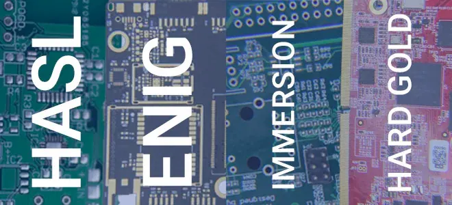
1. Pre‑inspection – Use a magnifying lamp or microscope to locate flux residues, solder balls, or particulate matter. Note areas with heavy buildup. 2. Solvent selection – Choose 90%+ IPA for rosin flux, a defluxer suited to no‑clean residues, or deionized water for water‑soluble flux. Verify compatibility with the board’s solder mask and surface finish (e.g., HASL, ENIG, OSP). 3. Application – Apply solvent via a spray bottle or a lint‑free wipe soaked in the liquid. Avoid pouring large volumes that could seep under components. 4. Gentle agitation – Lightly brush the area with a soft anti‑static brush or use a low‑pressure air blast to dislodge loosened residue. Do not scrub aggressively; mechanical stress can lift pads or damage thin copper. 5. Wipe‑dry – Use a fresh lint‑free wipe to remove dissolved residue and excess solvent. Change wipes frequently to prevent re‑depositing contaminants. 6. Rinse (if aqueous) – If using water‑based cleaning, rinse with fresh deionized water and then blow dry with filtered nitrogen or air. 7. Final dry – Allow the board to air dry in a clean environment or use a low‑temperature bake (e.g., 40 °C for 10 minutes) to evaporate any trapped solvent. 8. Visual check – Inspect again under magnification to confirm no residue remains.
Tools and Materials You Need
Having the right tools on hand makes the cleaning process repeatable and safe. Essential items include:
- Lint‑free wipes (polyester or cellulose) – non‑abrasive and low‑lint.
- Anti‑static brush with soft bristles – for gentle agitation.
- Spray bottles or pump bottles for controlled solvent application.
- Compressed air or nitrogen filtered to < 5 µm particles – for drying and blowing away debris.
- Magnification tools – 10×–20× loupe or a stereo microscope for inspection.
- Safety gear – nitrile gloves, safety goggles, and a fume hood or well‑ventilated area when using solvents.
Optional but useful for higher volume: a bench‑top ultrasonic cleaner set to a low frequency and mild detergent, or a vapor degreasing unit for large batches. Always verify that any equipment does not exceed the temperature or pressure limits of the board’s components.
Post‑Cleaning Inspection and Testing
After cleaning, perform a quick visual inspection to ensure no residue, discoloration, or lifting is present. Then move to electrical verification to confirm that the cleaning process did not introduce shorts or open circuits.
A simple first step is to check continuity between expected nodes using a multimeter. For detailed guidance, refer to using a multimeter to test your PCB board. Measure resistance between adjacent traces and pads; values should be in the megaohm range for unmated nets.
For high‑impedance or RF circuits, consider measuring insulation resistance with a megohmmeter or performing a time‑domain reflectometry (TDR) test if the equipment is available. These tests detect subtle leakage paths that a standard multimeter might miss.
If the board will undergo conformal coating, conduct a water break test or surface energy measurement to confirm the surface is sufficiently clean for coating adhesion. Finally, document the cleaning parameters (solvent type, exposure time, wipe count) in the production record to support traceability and continuous improvement.
Best Practices for Reliable Manufacturing
Integrate cleaning into the overall workflow rather than treating it as an isolated step. Define cleaning criteria in the work instructions based on flux type, component sensitivity, and required cleanliness class (e.g., IPC‑A‑610 Class 3). Train operators on proper solvent handling, wipe technique, and the importance of not re‑using contaminated wipes.
Periodically audit the cleaning process by performing witness coupons or test boards that are subjected to the same cleaning cycle and then inspected for residue. This helps detect drift in solvent effectiveness or equipment performance.
Partnering with an experienced EMS provider like Omini can provide access to validated cleaning procedures, specialized equipment, and process engineering support. Their expertise ensures that the cleaning step aligns with DFM guidelines, surface finish constraints, and the reliability targets of your product.
By treating PCB cleaning as a critical quality gate, you reduce the risk of latent defects, improve yields, and deliver electronics that perform consistently over their intended lifespan.
Related Omini Engineering Notes
- Custom PCB: The Most Important Part in Your Electronic Device
- Essential Steps for Effective PCB Board Testing