
Direct Answer
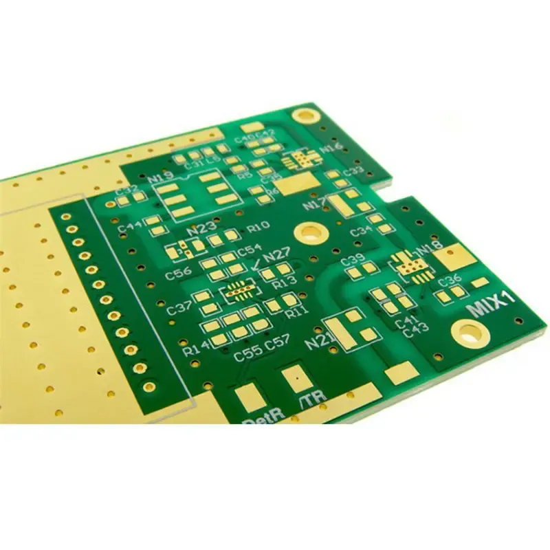
Successful microwave PCB fabrication starts with material selection and ends with rigorous high-frequency testing. Unlike standard digital boards, microwave circuits demand tight control over dielectric constant, loss tangent, and geometric precision to preserve signal integrity. Even small deviations in trace width, spacing, or substrate thickness can cause significant impedance shifts and phase errors at frequencies above 1 GHz. The process requires specialized laminates, precise etching, and validation techniques like TDR and VNA measurements to ensure performance matches simulation.
Omini supports microwave PCB projects by applying DFM checks tailored to high-frequency design rules and coordinating material sourcing with certified laminate suppliers. This foundational approach helps avoid costly redesigns and ensures the fabricated board meets both electrical and mechanical specifications.
Material Selection and Substrate Considerations
The substrate is the most critical factor in microwave PCB performance. Standard FR-4 exhibits high dissipation factor and variable Dk with frequency, making it unsuitable for applications above 1 GHz. Instead, engineers specify low-loss laminates such as Rogers RO4000 series, Taconic TLY, or Isola I-Tera MT40. These materials offer stable Dk values (typically 3.0–3.5) and low loss tangent (<0.004) across microwave bands.
Thickness tolerance is equally important. A 10% variation in dielectric thickness can shift impedance by 5–7%, which is unacceptable in 50-ohm systems. Fabricators must use precision-controlled prepreg and core layers, often measuring thickness via optical or beta-gauge methods during lamination. Copper foil selection also matters—reverse-treated or rolled annealed (RA) copper reduces conductor loss compared to standard electrodeposited (ED) foil, especially at millimeter-wave frequencies.
When reviewing Gerber files, confirm that the stackup notes specify the exact laminate type, thickness, and copper treatment. Any ambiguity here risks material substitution that could derail performance. Omini’s engineering team cross-checks Gerber notes against approved material lists during the pregs to prevent mismatches.
Stackup Design and Impedance Control
Symmetric stackup design is non-negotiable for microwave PCBs. Asymmetrical construction leads to warpage during thermal cycling, which alters trace geometry and introduces phase distortion. For multilayer boards, mirror the layer structure top-to-bottom: signal, ground, dielectric, power, dielectric, ground, signal. This balance minimizes bow and twist while maintaining consistent impedance references.
Controlled impedance traces require precise width and spacing calculations based on the laminate’s Dk and thickness. Use 2D field solvers (not just online calculators) for accuracy, especially with coplanar waveguide (CPWG) or grounded coplanar waveguide (GCPW) structures common in microwave design. Include solder mask and plating effects in simulations, as they can shift impedance by 2–4%.
Via design also impacts performance. Via-in-pad is often necessary for BGA or dense layouts but must be filled and plated over (via-in-pad plated over, or VIPPO) to avoid solder wicking and maintain surface planarity. Unfilled vias create discontinuities that act as shunt capacitors or inductors, degrading high-frequency response. Keep via stubs short or use back-drilled vias to eliminate resonance effects above 10 GHz.
DFM Checks for High-Frequency Designs
Standard DFM rules are insufficient for microwave PCBs. Focus on these high-frequency-specific checks:
- Trace width/spacing: Ensure minimum values account for etching undercut and plating buildup. A 6-mil trace designed for 50 ohms may etch to 5.2 mils, shifting impedance by 3–5%. Apply etching compensation factors in CAM.
- Annular ring: Maintain minimum 6-mil annular ring after plating to prevent breakout, especially with microvias. Thin rings increase resistance and can crack under thermal stress.
- Copper clearance: Increase clearance between traces and copper pours to avoid coupling and unintended stubs. A common mistake is pouring ground too close to signal lines, creating parasitic capacitance.
- Silkscreen placement: Keep silkscreen away from high-frequency traces and pads. Ink can slightly alter dielectric properties; avoid placing it within 10 mils of critical RF paths.
- Solder mask definition: Use non-solder mask defined (NSMD) pads whenever possible to maintain consistent pad size and reduce variability in assembly.
These checks are integrated into Omini’s CAM workflow, where automated flags highlight deviations from microwave-specific DFM thresholds before tooling begins.
Prototyping and Validation
Never skip high-frequency validation on prototypes. Time-domain reflectometry (TDR) reveals impedance discontinuities along traces, showing reflections from via stubs, bends, or width changes. Vector network analyzer (VNA) measurements confirm S11 (return loss) and S21 (insertion loss) match simulation targets across the operating band.
For example, a 10-GHz radar module might show -15 dB return loss in simulation but measure -8 dB on the first prototype due to via inductance. TDR would show a spike at each via location, guiding redesign—such as reducing via size or adding antipads.
Prototype panels should include test coupons with identical trace geometries to the actual RF paths. These coupons allow destructive testing (like peel strength) without sacrificing functional boards. Omini includes RF test coupon generation as part of its microwave PCB prototyping service, ensuring validation data is representative.
Surface Finish and Assembly Considerations
Surface finish affects both RF performance and solderability. Electroless nickel immersion gold (ENIG) is common but can cause signal loss at frequencies above 10 GHz due to nickel’s permeability. Alternatives like electroless nickel electroless palladium immersion gold (ENEPIG) or immersion silver offer lower loss while maintaining solderability.
Avoid organic solderability preservatives (OSP) for microwave boards exposed to multiple reflow cycles; OSP degrades quickly and offers no barrier against copper diffusion. For gold wire bonding applications, soft gold over nickel is standard, but thickness must be controlled to prevent cracking.
During assembly, use low-residue, no-clean fluxes to prevent ionic contamination that could increase loss tangent. Monitor reflow profiles closely—excessive time above Tg can delaminate low-loss laminates. X-ray inspection helps verify void-free solder joints under BGAs, which is critical for thermal and electrical performance in high-power RF applications.
Partnering for Microwave PCB Success
Microwave PCB fabrication is not a commodity process. It requires expertise in material science, high-frequency electromagnetics, and precision manufacturing. When selecting a partner, verify their experience with low-loss laminates, controlled impedance tracking, and RF validation capabilities.
Look for suppliers who routinely handle Rogers, Taconic, or similar materials and can provide traceability certificates. Ask about their DFM rule sets for high-frequency designs and whether they include TDR/VNA validation in prototyping.
Omini works with engineering teams to translate microwave design intent into manufacturable outputs, applying process controls that address the unique demands of high-frequency circuits. From Gerber review to final inspection, the focus remains on preserving signal integrity through every step of fabrication and assembly.
The key to success lies in treating microwave PCBs as precision RF components—not just printed boards. Material choice, stackup symmetry, trace geometry, and validation are interconnected. Weakness in any area compromises the whole system. By addressing each factor proactively and partnering with a fabricator who speaks the language of microwaves, engineers can achieve reliable performance from prototype to production.
Related Omini Engineering Notes
- Essential Factors to Consider When Choosing a PCB Fabrication Partner
- Essential PCB Design Guidelines for Beginners: A Step-by-Step Approach
- Essential Steps for Using a Multimeter to Test Your PCB Board
- Rigid-Flex PCB DFM Tips Before PCB Manufacturing
- Essential Tips for Finding a Trusted PCB Assembly Manufacturer in China