
Direct Answer
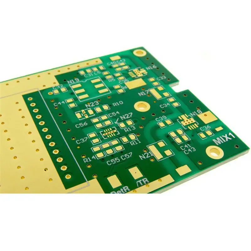
Teflon-based PCBs are engineered for high-frequency applications where signal loss, phase stability, and impedance control are critical. Made from polytetrafluoroethylene (PTFE) substrates, these boards offer exceptionally low dielectric loss and stable electrical properties up to 100 GHz and beyond, making them essential for RF, microwave, 5G, and aerospace systems.
Unlike standard FR-4, Teflon maintains consistent Dk and Df across frequency and temperature, minimizing signal distortion in high-speed digital and analog circuits. However, its non-stick surface and unique thermal expansion characteristics require specialized manufacturing processes, which we’ll explore in detail.
Why Teflon for High-Frequency Applications
The primary advantage of Teflon in PCBs lies in its electrical properties. PTFE has a dielectric constant (Dk) around 2.1–2.5 and a dissipation factor (Df) as low as 0.0002, which is nearly an order of magnitude better than FR-4. This results in minimal signal attenuation and phase shift, crucial for maintaining integrity in high-frequency signals.
In applications like 5G base stations, radar systems, and satellite communications, even small losses can degrade performance over long traces or complex routing. Teflon’s low loss tangent ensures that signals propagate with minimal energy dissipation, preserving amplitude and timing accuracy.
Thermal stability is another key benefit. Teflon substrates exhibit low coefficient of thermal expansion (CTE), often matching copper closely, which reduces stress on plated vias and interfaces during thermal cycling. This enhances reliability in harsh environments where temperature fluctuations are common.
However, these advantages come with manufacturing challenges. Teflon’s inert, non-stick surface resists adhesion, requiring surface treatment before lamination. Additionally, its low thermal conductivity can complicate heat dissipation in power-RF designs, necessitating thermal vias or metal cores in hybrid constructions.
Material Selection and Stackup Considerations
Choosing the right Teflon laminate involves balancing electrical performance, mechanical stability, and process compatibility. Pure PTFE offers the lowest loss but is soft and difficult to process. Filled variants—such as those with ceramic or glass microfibers—improve dimensional stability, rigidity, and copper bond strength while maintaining low Dk and Df.
Common Teflon-based laminates include Rogers RO3000 and RO4000 series, Taconic TLC and RF series, and Arlon AD and DiClad materials. Each is tailored for specific frequency ranges, power levels, and environmental conditions.
Stackup design must prioritize impedance control. Because Teflon’s Dk is lower than FR-4, trace widths for 50-ohm impedance are wider, which impacts routing density. Designers often use microstrip or stripline configurations with precise dielectric thickness control.
Via design also requires attention. Plated through-holes in Teflon PCBs can suffer from higher aspect ratio challenges due to the material’s softness. Blind and buried vias may be limited, and laser drilling is often preferred over mechanical drilling to avoid smearing and ensure clean hole walls.
For mixed-signal boards, hybrid stackups combining Teflon RF zones with FR-4 digital sections are common. This approach optimizes cost by using high-performance material only where needed. However, bonding dissimilar materials requires compatible prepregs and careful lamination cycles to prevent delamination.
Manufacturing Process Adaptations
Standard PCB fabrication processes must be adjusted for Teflon. The most critical step is surface preparation. Since PTFE resists adhesion, the copper-clad laminate undergoes plasma etching or chemical treatment (e.g., sodium naphthalene) to increase surface energy and enable reliable copper bonding.
Lamination cycles use lower temperatures and pressures compared to FR-4 to avoid deforming the soft PTFE core. Vacuum lamination is often employed to eliminate voids, and longer bake-out cycles may be needed to remove moisture absorbed during storage.
Drilling requires specialized parameters. High-speed carbide or diamond-tipped bits are used with reduced feed rates to prevent fraying or delamination. After drilling, desmear processes are adjusted—Teflon doesn’t smear like epoxy-based materials, but debris removal still requires tailored chemistry.
Copper plating follows standard electroless and electrolytic steps, but adhesion promoters may be added to the bath to enhance bond strength on the treated surface. Surface finishes like ENIG, immersion silver, or OSP are applied using standard lines, though adhesion testing is recommended.
Finally, electrical testing focuses on high-frequency parameters. Time-domain reflectometry (TDR) and vector network analyzer (VNA) scans verify impedance, insertion loss, and return loss across the design frequency range, ensuring the board meets RF performance targets.
Design for Manufacturability (DFM) Guidance
DFM for Teflon PCBs starts early in the design phase. Signal integrity simulations should include accurate Dk and Df values from the laminate supplier’s datasheet, not assumed FR-4 values. Tools like HyperLynx or SIwave, but require custom substrates, and CTE values to predict via stress and thermal behavior.
Panelization must account for material softness. Teflon panels are more prone to flex and vibration during handling, so larger tooling holes, stronger rails, or vacuum-assisted fixtures may be needed during assembly to prevent damage.
SMT assembly presents its own challenges. The low thermal conductivity of Teflon can lead to uneven heating during reflow, increasing the risk of tombstoning or insufficient solder paste melting. Adjusting reflow profiles—using longer soak zones or lower peak temperatures with extended time—helps achieve uniform heating.
Component placement accuracy is critical, especially for fine-pitch BGAs and RF connectors. Fiducial marks should be placed on stable areas, and vision systems may need adjusted lighting due to Teflon’s low reflectivity.
Finally, partner with a manufacturer experienced in high-frequency materials. Omini supports Teflon PCB projects with DFM review, material certification, process validation, and RF testing to ensure your design transitions smoothly from prototype to production.
Applications in RF, Microwave, and 5G Systems
Teflon PCBs are widely used in systems where signal fidelity is non-negotiable. In 5G infrastructure, they power antenna arrays, beamforming networks, and high-speed interconnects between RFICs and baseband processors. The low loss enables efficient power transmission and minimizes heat generation in active components.
Radar systems—both automotive and aerospace—rely on Teflon for transmit/receive modules, phase shifters, and waveguide transitions. The material’s stability over temperature ensures consistent beam pointing and detection accuracy across environmental extremes.
Satellite communications and space payloads use Teflon for its outgassing performance (when properly certified) and radiation stability. Combined with proper conformal coating or hermetic sealing, Teflon PCBs maintain functionality in vacuum and thermal cycling conditions.
Test and measurement equipment, such as oscilloscopes and signal generators, also benefit from Teflon’s precision. Internal RF paths, reference oscillators, and calibration networks require the phase stability and low jitter that only low-loss substrates can provide.\n As frequencies push into millimeter-wave bands (30–300 GHz), the advantages of Teflon become even more pronounced. At these wavelengths, even minor discontinuities or loss mechanisms degrade performance rapidly, making material choice a first-order design decision.
Closing Notes
Working with Teflon PCBs demands attention to material behavior, process adaptation, and RF-aware design. It’s not just about selecting a low-loss substrate—it’s about understanding how that material interacts with every step of manufacturing, from surface treatment to final test. For teams pushing into higher frequencies or tighter tolerances, the investment in proper material handling and process control pays off in yield, reliability, and signal integrity. If your next RF or microwave project is hitting performance walls with standard materials, it’s worth evaluating whether a Teflon-based approach—supported by a partner who knows the nuances—can unlock the next level of performance.
Related Omini Engineering Notes
- PCB Stack-Up and Signal Integrity for High-Speed Boards
- Commonly Used Rigid PCBs and Rigid PCB Materials
- Decoding High-Density Interconnect (HDI) PCB Technology: An Overview
- Double Sided PCB: Advantages, Applications, and Manufacturing Process
- Circuit Board Manufacturing Process: A Comprehensive Guide for Beginners