
Direct Answer
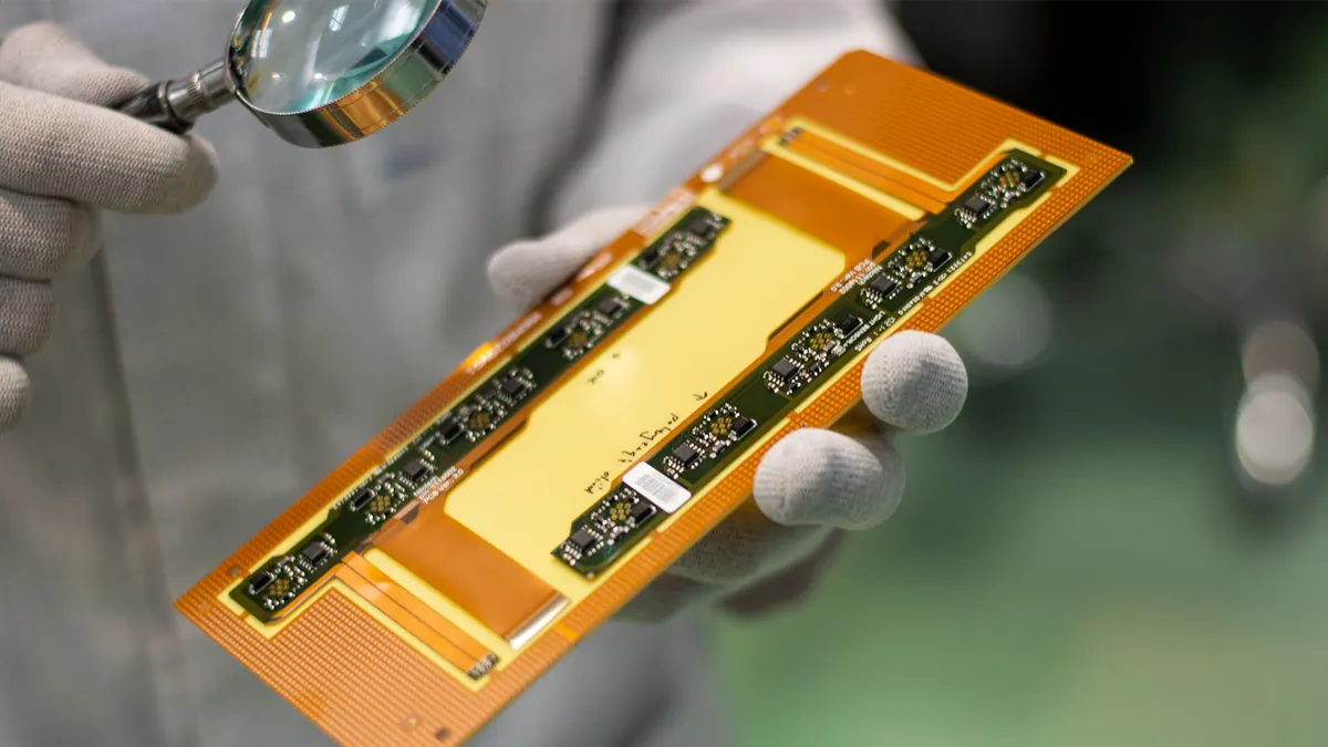
Flex PCB manufacturing transforms polyimide-based substrates into reliable, bendable circuits used in wearables, medical devices, and aerospace systems. Unlike rigid boards, the process accommodates material flexibility through specialized handling, laser-based via formation, and coverlay protection instead of traditional solder mask.
This overview walks beginners through each stage — from material selection and design rules to fabrication, testing, and final inspection — highlighting where design decisions impact manufacturability and long-term performance.
Material Selection and Substrate Preparation
The foundation of any flex PCB is its dielectric substrate, most commonly polyimide (e.g., Kapton®) for its excellent thermal stability, chemical resistance, and mechanical flexibility. Thickness typically ranges from 12.5 to 50 microns, chosen based on bend requirements and mechanical stiffness.
Copper foil, usually electrodeposited or rolled annealed (RA), is laminated to the polyimide using either adhesive or adhesiveless methods. Adhesiveless constructions bond copper directly to polyimide, reducing thickness and improving flex endurance — critical in dynamic applications like folding smartphones or implantable devices.
Before processing, substrates undergo cleaning and surface activation to ensure strong adhesion during plating and lamination. Any contamination can lead to delamination or poor via formation, so strict environmental controls are maintained in cleanroom-rated areas.
Imaging and Circuit Formation: From Gerber to Copper Pattern
The manufacturing process begins with Gerber files, which define the copper traces, pads, and vias. These are used to create a phototool or directly drive a laser imaging system. A photosensitive dry film or liquid photoresist is applied to the copper-clad substrate, then exposed to UV light through the mask.
After exposure, the resist is developed, leaving a pattern that protects copper during etching. Chemical etchants (typically ammoniacal or alkaline copper chloride) remove exposed copper, leaving only the desired circuit traces. Precision is vital — underetching causes shorts, while overetching narrows traces and increases resistance.
For fine-line designs common in HDI flex circuits, laser direct imaging (LDI) improves resolution and registration accuracy, reducing the risk of misalignment between layers in multilayer flex or rigid-flex stacks.
Via Formation: Laser Drilling and Plating
Vias in flex PCBs are almost exclusively formed using laser drilling — typically UV or CO2 lasers — which can precisely ablate through polyimide and copper without damaging surrounding material. This enables microvias as small as 50 microns, essential for high-density interconnects.
After drilling, holes are cleaned and desmeared to remove resin debris. A thin conductive layer is then deposited via electroless copper plating, followed by electrolytic plating to build up sufficient thickness for electrical continuity and mechanical strength.
In rigid-flex designs, vias may transition from rigid to flex zones, requiring careful stackup planning to manage stress points. This is where DFM checks become essential — ensuring via placement avoids high-strain areas and that annular rings are sufficient to withstand flexing.
For deeper guidance on designing rigid-flex circuits with manufacturability in mind, see our guide on Rigid-Flex PCB DFM Tips Before PCB Manufacturing.
Coverlay Lamination and Surface Protection
Instead of solder mask, flex PCBs use a coverlay — a laminated polyimide sheet with an adhesive layer — to protect circuitry. Openings in the coverlay align with pads and vias, exposing them for component attachment or testing.
The coverlay is applied under heat and pressure in a vacuum lamination process to eliminate bubbles and ensure uniform adhesion. Adhesiveless coverlay options, where the polyimide bonds directly to the cured adhesive layer, are preferred in high-reliability applications to reduce outgassing and improve thermal performance.
Surface finishes are then applied to exposed pads. Common options include ENIG (electroless nickel immersion gold), OSP (organic solderability preservative), and HASL (hot air solder leveling). ENIG is often chosen for flex due to its flat surface and compatibility with fine-pitch components, though OSP may be used for cost-sensitive, short-term applications.
To understand how these finishes compare in real-world production, review our breakdown of ENIG vs OSP vs HASL for PCB Manufacturing.
Cutting, Punching, and Final Shaping
Unlike rigid PCBs routed with mechanical bits, flex circuits are typically cut using precision punching dies or laser systems. Steel rule dies are cost-effective for high-volume shapes, while lasers offer flexibility for prototypes or complex geometries without tooling changes.
The cutting process must maintain positional accuracy to avoid damaging traces near the edge. After cutting, panels may undergo additional stiffener attachment — usually FR4 or polyimide — in areas requiring rigidity for connector mounting or component support.
Stiffeners are bonded using thermal or pressure-sensitive adhesives, and their placement is critical: too close to a bend point can create a stress riser, leading to premature failure.
Electrical and Reliability Testing
Every flex PCB undergoes electrical testing to verify continuity and isolation. Flying probe or fixture-based testers check for opens, shorts, and resistance values against netlist data from the Gerber files.
For dynamic applications, flex cycling testing is mandatory. Samples are bent repeatedly — often thousands of cycles — at a defined radius while monitoring electrical continuity. Standards like IPC-TM-650 2.4.1 provide guidelines for test duration, radius, and failure criteria.
Additional tests may include:
- Peel strength: measures adhesion between copper and polyimide
- Dielectric withstanding voltage: validates insulation integrity
- Humidity and thermal cycling: assesses environmental stability
These tests are especially important in medical, automotive, and aerospace contexts where failure is not an option.
Design Considerations That Impact Manufacturability
Several design choices directly affect yield and reliability in flex PCB production:
- Bend radius: Keep traces at least 10x the substrate thickness from the neutral bend axis
- Trace routing: Use staggered, not stacked, traces in dynamic zones to distribute strain
- Via placement: Avoid placing vias in high-flex areas; use teardrop pads to reduce stress concentration
- Pad size: Maintain sufficient annular ring after plating to withstand flex-induced movement
- Stiffener placement: Locate stiffeners to support connectors without restricting flex
Addressing these early in design — ideally during Gerber/BOM review — reduces rework and improves first-pass yield. For a broader look at PCB fabrication fundamentals, see our guide on Double Sided PCB: Advantages, Applications, and Manufacturing Process.
Applications Where Flex PCBs Excel
Flex PCBs enable solutions where rigid boards fail:
- Wearables: Conform to body contours and withstand repeated flexing
- Medical devices: Fit in minimally invasive tools and implantable electronics
- Aerospace: Reduce weight and absorb vibration in tight spaces
- Consumer electronics: Enable folding displays, camera modules, and sliding mechanisms
- Automotive: Used in steering wheels, sensors, and LED lighting under constant vibration
In each case, the ability to dynamically bend or fold while maintaining electrical integrity is the key advantage.
Working With an Experienced Manufacturer
Flex PCB manufacturing demands precision in material handling, process control, and testing. For Omini RFQs, the practical requirement is to define the flex stackup, bend radius, stiffener plan, inspection scope, and validation evidence before production release.
From early DFM feedback to final validation, engineering support should turn flex circuit concepts into producible designs, especially for applications where performance under flex is non-negotiable.
For teams exploring embedded circuitry within flex or rigid-flex assemblies, our guide on Embedded PCB: A Comprehensive Guide for Beginners provides foundational insights.
Circuit Board Manufacturing: The Broader Context
Understanding flex PCB production is easier when viewed within the full electronics manufacturing flow. From schematic capture and BOM validation to SMT assembly and final test, each step depends on accurate, manufacturable designs.
For a complete walkthrough of how PCBs move from fab to finished assembly, refer to our detailed overview of the Circuit Board Manufacturing Process: A Comprehensive Guide for Beginners.
Flex circuits continue to push the boundaries of miniaturization and motion in electronics. Success starts with respecting the material’s limits, designing for flex from the outset, and validating every stage — from laser-drilled via to final flex cycle — with rigor and clarity.