
Direct Answer
Circuit board manufacturing is the sequence of transforming electronic design data into a functional assembled product. The process splits into two major phases: fabrication (creating the bare PCB with copper traces, vias, and solder mask) and assembly (mounting and soldering components to create a PCBA). For beginners, the critical insight is that decisions made during design and sourcing—stack-up, material selection, component availability, and test strategy—determine cost, lead time, and reliability far more than any single production machine.
A typical project flows through DFM review, bare board fabrication, component procurement, SMT/THT assembly, inspection, testing, and final packaging. Each stage has failure modes that compound if not caught early. The following sections walk through what actually happens on the factory floor and where teams commonly lose time or money.
From Design Data to Fabrication Ready
Before any copper is etched, a manufacturing partner validates that the design files are buildable. This step—DFM and DFA review—catches issues that CAD tools often miss: trace-to-pad spacing below fabricator limits, unplated holes in critical locations, copper pour slivers, or asymmetric stack-ups that warp during reflow.
Engineers submit Gerber RS-274X files, drill data, netlists, and fabrication notes. A competent EMS service model partner will flag impedance control requirements, controlled depth drilling needs, or HDI blind/buried via feasibility. At Omini, this review typically surfaces 3–5 issues per new design—missing solder mask dams between fine-pitch pads, insufficient annular rings, or non-standard material calls that extend lead times. Fixing these digitally avoids scrap, rework, and schedule slips.
Stack-Up and Material Selection
The PCB substrate choice—FR-4, high-Tg FR-4, polyimide, or Rogers—sets thermal performance, signal integrity, and cost ceilings. For standard IoT or industrial controllers, mid-Tg FR-4 with standard copper weights suffices. For RF, automotive, or high-reliability applications, material selection cascades into drilling parameters, plating chemistry, and final surface finish choices (ENIG, OSP, immersion tin, or HASL).
Beginners often underestimate how stack-up decisions in design tools translate to real laminate procurement. Exotic materials have longer lead times and stricter processing windows. If your design does not truly need Rogers 4350B, specifying it adds weeks and cost without benefit.
Bare PCB Fabrication: Layer by Layer
Fabrication builds the board through additive and subtractive processes. Understanding the sequence helps teams diagnose quality issues and set realistic expectations.
Imaging, Etching, and Layer Registration
Inner layers are printed with photoresist, exposed to the design pattern, and etched to leave copper traces. Multiple layers are laminated with prepreg (pre-impregnated resin) and core materials, then pressed under heat and pressure. Registration—aligning layers precisely—is where multilayer boards fail most often. Misregistration causes open circuits, shorts, or weakened vias.
Drilling and Plating
Mechanical drills create through-holes; laser drills create microvias in HDI designs. After drilling, a chemical process deposits thin electroless copper, followed by electrolytic copper plating to achieve target wall thickness. Plating uniformity matters: thin spots in high-aspect-ratio vias create reliability risks under thermal cycling.
Solder Mask, Silkscreen, and Surface Finish
Solder mask (typically green, but available in any color) insulates copper and defines where solder will wet. Silkscreen adds component identifiers and polarity marks. Surface finish protects exposed copper until assembly. ENIG (electroless nickel immersion gold) dominates for fine-pitch SMT due to flatness and shelf life. OSP is cheaper but less robust for multiple thermal cycles.
Component Sourcing: The Hidden Schedule Driver
While bare boards fabricate in parallel, component procurement often determines the true critical path. A BOM Risk Strategy for Turnkey PCB Assembly is essential in today's allocation environment.
BOM Scrubbing and Alternates
A clean BOM lists manufacturer part numbers, descriptions, quantities per board, and reference designators. Experienced buyers cross-check lifecycle status, stock depth Worldwide, and second-source options. For allocated parts, engineering may need to qualify alternates—a process that can take days or weeks depending on testing requirements.
Consignment vs. Turnkey Tradeoffs
In turnkey arrangements, the Manufacturing capabilities overview of your partner determines how much sourcing leverage they bring—volume pricing, preferred supplier relationships, and allocation priority. Consignment gives OEMs component cost control but shifts sourcing burden and liability to their team. Hybrid models split strategic long-lead parts (consigned) from commodity passives (turnkey).
SMT Assembly: The Heart of PCBA
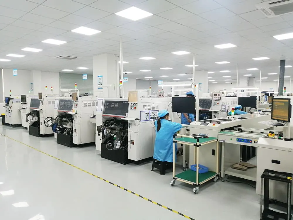
Surface mount technology dominates modern assembly. Components are placed by high-speed pick-and-place machines and soldered in reflow ovens.
Stencil Printing and Paste Inspection
Solder paste is deposited through a laser-cut stainless steel stencil onto pads. Paste volume, alignment, and consistency are checked by solder paste inspection (SPI). Poor printing causes the majority of SMT defects—insufficient paste leads to opens; excess paste causes bridging.
Placement and Reflow
Chip shooters place small passives at rates exceeding 80,000 components per hour. Larger ICs, connectors, and odd-form parts follow on flexible-placement gantries. The populated board enters a reflow oven with a carefully profiled temperature curve: preheat, soak, reflow above liquidus, and cooling. Profile optimization prevents tombstoning, voiding, and component damage.
Through-Hole and Mixed Technology
Not all components suit SMT. Large connectors, transformers, and some high-power devices require through-hole insertion followed by wave soldering or selective soldering. Mixed-technology boards need process sequencing—typically SMT first, then THT—to avoid thermal damage to already-soldered components.
Inspection and Quality Gates
Catching defects before they ship is cheaper than field failures. Modern assembly lines use multiple inspection layers.
AOI and X-Ray Inspection in PCB Assembly describes how automated optical inspection catches visible defects—missing components, wrong polarity, solder bridging—while X-Ray penetrates QFN, BGA, and connector solder joints where optical access is impossible. Together with in-circuit test (ICT) and functional test, these methods form a defense-in-depth strategy that protects yield and reliability.
For high-reliability products, additional screening like thermal cycling, vibration test, or burn-in may apply. The key is matching test coverage to product risk: consumer electronics rarely justify the same rigor as automotive or medical devices.
Testing, Programming, and Final Integration
After soldering and inspection, assembled boards often require firmware programming, calibration, or boundary scan verification. These steps happen on dedicated test fixtures or flying probe systems. Programming errors, incorrect firmware revisions, or calibration drift are common pitfalls that escape detection without systematic test protocols.
Final integration—adding enclosures, cables, labels, and packaging—completes the manufacturing value chain. A partner with full EMS service model capabilities can manage this as a single workflow rather than fragmented handoffs.
Cost Structure and Optimization Levers
Understanding cost drivers helps teams make informed tradeoffs. PCB Assembly Cost Optimization: Engineering Margin Back Into Your Build explores how design choices—panelization, component standardization, test strategy—affect landed cost.
At a high level, bare PCB cost scales with layer count, board size, material, and drill complexity. Assembly cost scales with component count, mix of SMT vs. THT, single vs. double-sided placement, and test coverage. NRE charges apply for stencils, fixtures, and programming. Volume breaks are significant: moving from 100 to 10,000 units typically reduces per-unit assembly cost by 30–50%.
Beginners often over-specify tolerances or materials, assuming tighter is always better. In practice, manufacturing to standard tolerances with robust design rules yields higher first-pass yield at lower cost.
What to Look for in a Manufacturing Partner
Not all EMS providers are equivalent. Evaluate partners on:
- Technical depth: Can they build your stack-up and component mix? Do they offer DFM feedback or merely execute?
- Quality systems: What inspection equipment is in-line? What traceability systems track lots and materials?
- Supply chain agility: How do they handle allocation, alternates, and long-lead parts?
- Communication: Do they provide clear status updates, or do projects disappear into opaque black boxes?
Omini operates as a manufacturing partner across these dimensions, supporting clients from prototype through volume with transparent process control and engineering engagement.
Field Notes for Your First Build
If you are new to circuit board manufacturing, start by treating your first build as a learning cycle, not a finished process. Send your design package early for DFM review. Validate your BOM against real distributor stock before finalizing a schedule. Build a small pilot lot to discover assembly issues—stencil aperture problems, component orientation ambiguities, or thermal sensitivities—before committing to volume.
The teams that move fastest are not necessarily the ones with the most experience, but those that build feedback loops between design, sourcing, and production. Every defect type you catalog, every alternate you qualify, and every profile you optimize compounds into faster, cheaper, more reliable builds down the line. That is the real skill in circuit board manufacturing: not knowing every machine parameter, but knowing how to close the loop between what you designed and what the factory can repeatedly build.