
Direct Answer
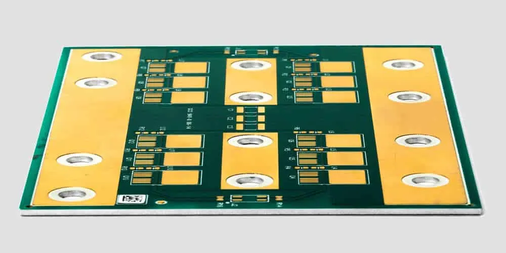
Copper core PCBs replace the traditional FR4 substrate with a solid copper or aluminum base layer, fundamentally changing how a board manages heat. Instead of routing heat through vias to a separate heatsink, the copper core itself becomes the primary thermal path—drawing heat directly from components and spreading it across the entire board surface. This construction is especially valuable in high-power electronics where thermal failure modes like solder joint fatigue, LED lumen depreciation, and semiconductor junction breakdown determine product lifespan.
For electronics manufacturing services (EMS) providers and OEM partners, copper core technology sits at the intersection of material science, thermal design, and process control. The decision to specify a metal-core board triggers changes across the manufacturing chain: from stack-up design and dielectric selection through SMT reflow profiling, inspection protocols, and final reliability testing. Understanding these interdependencies is critical for any EMS service model that supports power electronics or thermally challenged applications.
How Copper Core PCBs Work: The Thermal Path
Standard FR4 boards are thermal insulators. Heat generated by components must travel through the PCB thickness—typically poor at conducting heat—then spread laterally or transfer to an external heatsink through vias or thermal pads. This path adds thermal resistance, creates hot spots, and often demands bulky mechanical solutions.
Copper core PCBs invert this logic. A typical insulated metal substrate (IMS) construction layers a thin copper foil circuit layer over a thermally conductive dielectric, which bonds to a thick copper or aluminum base. The dielectric—usually epoxy or polyimide filled with ceramic particles like aluminum oxide or boron nitride—provides electrical isolation while conducting heat vertically. The metal base then spreads that heat laterally with the high thermal conductivity of copper (approximately 400 W/mK) or aluminum (approximately 200 W/mK).
The result is a dramatic reduction in junction-to-case thermal resistance for power components. A MOSFET or LED mounted on a copper core board can operate at significantly lower temperatures than the same component on FR4 with identical ambient conditions. This matters concretely: for every 10°C reduction in junction temperature, semiconductor lifetime approximately doubles.
The tradeoff is mechanical and electrical. The metal core adds weight, limits via construction options, and requires careful handling of galvanic corrosion between dissimilar metals. Dielectric thickness must balance thermal performance against breakdown voltage requirements. These constraints make material selection a collaborative exercise between the OEM designer and the manufacturing partner.
Material Variants and Selection Criteria
Not all copper core boards are interchangeable. The manufacturing partner must match the substrate construction to the application's thermal, electrical, and mechanical demands.
Insulated Metal Substrates (IMS)
IMS remains the most common copper core format for medium-power applications. The ceramic-filled dielectric layer typically ranges from 75 to 150 microns thick, with thermal conductivity from 1.0 to 3.0 W/mK. Higher conductivity dielectrics cost more but enable thinner layers for equivalent thermal performance, improving mechanical flexibility and reducing drill aspect ratios for vias.
The dielectric's thermal impedance—not just conductivity—determines real-world performance. A thin, moderate-conductivity layer often outperforms a thick, high-conductivity layer because the total thermal resistance depends on thickness divided by conductivity. Experienced EMS teams work backward from the component's maximum junction temperature and required operating ambient to specify the right dielectric rather than defaulting to the highest conductivity available.
Direct Bond Copper (DBC) and Active Metal Brazing (AMB)
For the highest power densities—electric vehicle inverters, traction drives, industrial welding equipment—ceramic substrates with directly bonded copper layers replace organic dielectrics entirely. Alumina (Al₂O₃), aluminum nitride (AlN), or silicon nitride (Si₃N₄) ceramic cores offer thermal conductivity from 24 to 170 W/mK with excellent electrical isolation and high-temperature capability.
These substrates demand fundamentally different fabrication processes. The ceramic is brittle, requiring specialized scoring and breaking rather than routing. Copper foil thicknesses are typically 0.25 to 0.30 mm, enabling high current capacity but complicating fine-pitch etching. Assembly moves from standard SMT toward die-attach, wire bonding, or sintering processes. Most generalist EMS providers do not handle DBC/AMB in-house, making supply chain qualification critical.
Thermal Conductivity vs. Electrical Isolation
A practical tension in copper core design is that better thermal conductors tend to be worse electrical insulators. The ceramic-filled epoxies in IMS trade some conductivity for reliable dielectric strength. Ceramic substrates invert this: excellent in both dimensions but expensive and fragile. For a given design, the right choice depends on working voltage, creepage requirements, mechanical shock tolerance, and cost targets. A capable manufacturing partner guides this tradeoff with empirical data rather than catalog specifications alone.
Manufacturing Process Considerations
Copper core fabrication diverges from standard PCB processing at multiple points. Understanding these differences prevents yield loss and field failures.
Lamination and Drilling
The metal core's presence prevents through-hole plating of the type used in multilayer FR4. Vias must be mechanically isolated from the core—typically by drilling oversized holes, filling with non-conductive epoxy, and then drilling and plating the signal via. This blind via construction adds cost and limits routing density. Some designs use microvias laser-drilled through only the top copper and dielectric layer, landing on the metal core, but these require careful control of dielectric thickness and laser parameters.
Board warpage during lamination is another concern. The coefficient of thermal expansion (CTE) mismatch between copper (17 ppm/°C) and typical dielectrics (50-70 ppm/°C) creates internal stress. High-temperature lamination cycles must be controlled to prevent delamination or residual bow that complicates later assembly.
SMT Reflow Profile Engineering
The most immediate assembly challenge is thermal mass. A 2.0 mm copper core board absorbs significantly more heat than a 1.6 mm FR4 board, demanding extended reflow profiles. A standard lead-free profile with 60-90 second soak and 60-90 second reflow may need 30-50% more time above liquidus to ensure complete solder joint formation on large thermal pads.
The risk is overheating smaller components while bringing the thermal pad to temperature. Uneven heating across the board can also stress solder joints differentially. Advanced EMS providers use multi-zone ovens with profiling boards embedded with thermocouples at critical locations—component bodies, thermal pads, board edges—to validate that every location sees acceptable temperatures without exceeding component limits.
For mixed-technology boards with both power devices on copper core areas and signal components on conventional substrate, selective reflow or step-stencil printing may be necessary. The Circuit Board Manufacturing Process: A Comprehensive Guide for Beginners covers how these process decisions cascade through the manufacturing plan.
Inspection and Reliability Testing
Standard AOI faces limitations with reflective copper surfaces and the high-aspect-ratio solder joints common on thermal pads. X-ray inspection becomes essential for verifying void-free solder attachment beneath power components, where even small voids create localized hot spots. The article on AOI and X-Ray Inspection in PCB Assembly details how these methods complement each other for metal-core boards.
Thermal cycling reliability testing must account for the different CTE of copper core constructions. IPC-TM-650 methods apply, but failure modes shift: dielectric delamination at the copper interface, solder fatigue at component-to-board interfaces due to CTE mismatch, and conductive anode filament (CAF) growth in the presence of moisture and bias. A rigorous incoming material qualification and lot traceability system, such as that described in BOM Risk Strategy for Turnkey PCB Assembly, helps isolate whether field failures stem from material, process, or design root causes.
Design for Manufacturability on Metal-Core Substrates
DFM for copper core boards extends beyond standard PCB rules. Several patterns recur in successful designs.
Thermal Pad and Stencil Design
Power components on copper core boards typically use large exposed thermal pads rather than individual leads for heat transfer. Stencil design must balance solder volume—enough to fill the pad and eliminate voids, but not so much that bridging occurs or the component floats during reflow. Common approaches include window-pane apertures with 50-70% coverage, or dot-matrix patterns that vent flux gases during reflow.
The solder paste specification also matters. Higher-activity flux systems may be needed for the extended reflow profiles, but residues must be compatible with any conformal coating or potting. No-clean pastes predominate, but the specific chemistry should be validated against the dielectric material for compatibility.
Component Placement and Spacing
Large copper areas near small passive components create thermal gradients that affect solder paste behavior. A resistor near a power MOSFET's thermal pad may see premature flux activation or dry-out. Spacing rules and thermal relief patterns must account for these interactions. Similarly, components on the opposite side of a single-sided copper core board experience different thermal conditions than in standard double-sided FR4 construction.
Mechanical Attachment and Enclosure Integration
Copper core boards often mount directly to an enclosure or chassis for additional heat sinking. This requires planning for mounting holes, standoff heights, and thermal interface materials. The board fabricator must hold tight tolerances on hole locations and board thickness to ensure proper thermal contact without stressing solder joints. Threaded inserts or PEM nuts may be specified, requiring coordination between PCB fabrication and final assembly processes.
For designers comparing substrate options, Comparing Different Types of Printed Circuit Board Materials provides additional context on how copper core fits within the broader material landscape.
When to Specify Copper Core: A Decision Framework
Copper core adds cost and complexity. It is not the default choice but rather a targeted solution for specific thermal constraints.
Consider copper core when: component power dissipation exceeds what FR4 can manage without external heatsinks; the product envelope prohibits heatsinks or airflow; thermal cycling reliability is critical and solder joint fatigue is a dominant failure mode; or the application requires extremely uniform board temperature (some optical and RF applications).
Avoid or reconsider when: the design requires multilayer complexity with blind and buried vias that metal-core construction cannot accommodate; weight is severely constrained (aluminum core may substitute but with thermal penalty); or cost targets are tight and thermal requirements can be met with conventional means.
The transition point is often empirical. A rule of thumb: when calculated junction temperatures with FR4 exceed 85-90% of rated maximums with margin for ambient variation and aging, copper core warrants serious evaluation. Thermal simulation with realistic board models, not just component-level calculations, informs this decision.
Working with an EMS Partner on Copper Core Programs
Copper core PCB programs benefit from early manufacturing partner involvement. Material availability varies by region and lead time; dielectric formulations from different suppliers perform differently despite similar specifications; and process windows are narrower than for standard FR4.
Omini approaches copper core projects with the same methodology applied across its EMS programs: collaborative DFM review, transparent process definition, and traceable execution. The engineering team validates reflow profiles against actual board constructions, not generic recipes, and maintains qualification data across dielectric suppliers to mitigate material availability risks. For OEMs transitioning from FR4 to metal-core designs, this manufacturing partnership model reduces the learning curve and catches thermal-mechanical issues before they reach volume production.
The supply chain dimension is equally important. Copper core substrates have longer lead times than commodity FR4 and fewer qualified suppliers globally. A manufacturing partner with established material relationships and buffer stock strategies, aligned with the principles in BOM Risk Strategy for Turnkey PCB Assembly, protects program schedules from substrate availability constraints.
Field Notes: What Separates Successful Deployments
After reviewing hundreds of copper core programs, certain patterns distinguish successful implementations from problematic ones. Designs that treat the copper core as merely a "better heatsink" without adjusting the electrical and mechanical design tend to struggle. Those that redesign the thermal path from component to ambient—considering the board as an active thermal element, not just a wiring substrate—achieve the reliability and performance gains that justify the technology.
The most common avoidable failure is inadequate solder joint verification beneath power components. Standard visual inspection and even some AOI configurations miss voids in thermal pad solder joints. X-ray inspection with void analysis, specified in the quality plan from program launch, catches these before boards ship.
Another pattern: assuming that copper core eliminates all thermal concerns. It improves the board-level path but does not change the need for adequate enclosure ventilation, proper thermal interface materials at system interfaces, and realistic operating environment specifications. The best copper core design still fails in an unventilated enclosure at 85°C ambient.
For teams building the next generation of power-dense electronics, copper core PCBs offer a proven path to manage heat without proportional growth in system size or cost. The technology rewards careful engineering and disciplined manufacturing partnership with measurable gains in reliability, performance, and product longevity.
Related Omini Engineering Notes
- Circuit Board Manufacturing Process: A Comprehensive Guide for Beginners
- Comparing Different Types of Printed Circuit Board Materials
- EMS service model
- BOM Risk Strategy for Turnkey PCB Assembly
- AOI and X-Ray Inspection in PCB Assembly