
Direct Answer
The world’s largest PCB manufacturers are defined not just by factory size, but by their ability to deliver complex, high-reliability boards at scale while maintaining tight tolerances and consistent yield. These companies invest heavily in automation, advanced imaging, and surface finish technologies to serve markets like 5G infrastructure, electric vehicles, and aerospace systems. Their scale allows them to absorb R&D costs for next-gen processes such as sequential lamination for HDI or laser-drilled microvias, which smaller shops may struggle to justify.
For engineering teams and procurement specialists, understanding where these leaders excel—whether in rigid-flex for dynamic assemblies, high-layer-count server boards, or impedance-controlled RF substrates—helps match project needs with the right manufacturing partner. This isn’t about picking the biggest name, but aligning technical capabilities with design requirements, volume expectations, and quality standards.
Technological Leadership in HDI and Rigid-Flex
At the forefront of innovation, the top PCB manufacturers push boundaries in high-density interconnect (HDI) and rigid-flex technologies. HDI boards, featuring microvias, blind/buried vias, and fine-line patterning, are essential for smartphones, wearables, and advanced driver-assistance systems (ADAS). Leaders like Unimicron and AT&S have developed proprietary processes for laser via formation and sequential build-up that enable layer counts of 12+ with tight pitch control.
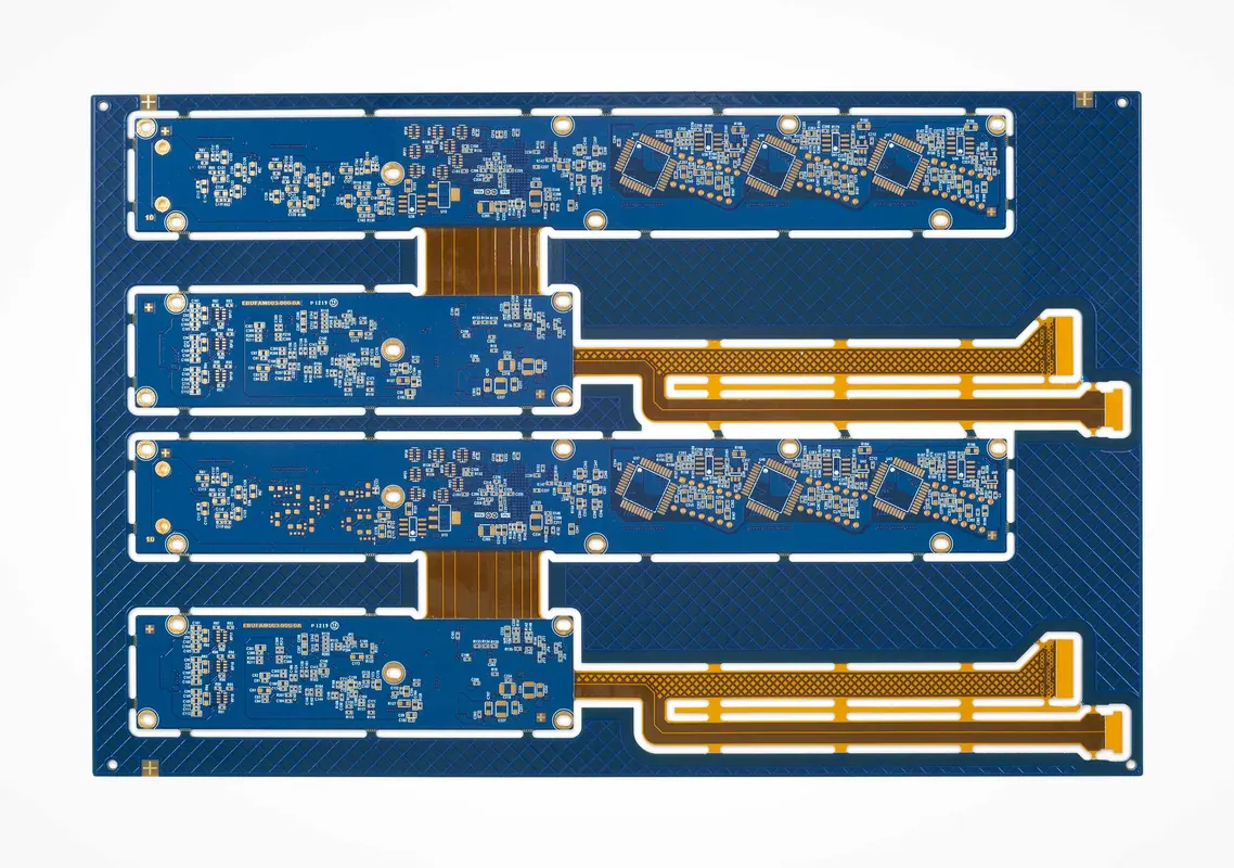
Rigid-flex PCBs, which combine rigid sections for component mounting with flexible circuits for dynamic interconnects, require precise lamination control to prevent delamination or cracking under flex cycles. Manufacturers with dedicated rigid-flex lines use specialized adhesives and temperature-controlled presses to support bond strength. Buyers should verify that any rigid-flex RFQ includes bend radius, stackup, material, inspection, and test requirements before production release.
These capabilities aren’t just about complexity—they directly impact signal integrity, thermal performance, and mechanical durability. A manufacturer’s depth in these areas often determines whether a design can transition from prototype to volume production without redesign.
Global Footprint and Supply Chain Resilience
The largest PCB manufacturers operate across multiple continents, with major facilities in Taiwan, China, South Korea, Vietnam, and increasingly in Europe and North America. This geographic spread isn’t just for cost optimization—it’s a strategic response to trade tensions, natural disasters, and pandemic-related disruptions. For example, a company with fabs in both Taiwan and Vietnam can shift production if one region faces typhoon-related delays or export restrictions.
This resilience matters for OEMs managing long product lifecycles. A shift in sourcing from one region to another requires consistent process control and documentation. Leading manufacturers maintain global quality systems (often IATF 16949, AS9100, or ISO 13485 certified) so that a board made in Malaysia matches the spec of one made in China. This consistency reduces qualification burden when dual-sourcing or shifting volume.\n For Omini buyers, the relevant lesson is different: confirm where the manufacturing work is controlled, which factory records are available, and how component availability, lead time, quality evidence, and shipment handoff are handled before release.
High-Reliability Focus: Aerospace, Medical, and Defense
While consumer electronics drive volume, the highest margins and most stringent requirements come from aerospace, medical, and defense sectors. These markets demand PCBs that withstand extreme temperatures, vibration, radiation, or long-term storage. The largest manufacturers have dedicated lines for high-reliability builds, using materials like polyimide, PTFE laminates, or copper invar for CTE matching.
Surface finish selection becomes critical here—ENIG remains common for its flatness and solderability, but immersion silver or OSP may be chosen for specific RF or cost constraints. For high-reliability applications, manufacturers often recommend electrolytic nickel gold over ENIG for better corrosion resistance, especially in humid or salt-spray environments.
Stackup design also plays a key role. Controlled impedance, buried capacitance layers, and thermal vias for heat dissipation are standard in radar modules or implantable devices. Manufacturers with strong engineering teams work closely with customers during DFM review to optimize stackup for both electrical performance and manufacturability—avoiding issues like resin starvation or uneven copper distribution.
Omini's RFQ workflow should connect these considerations to the PCBA plan so the PCB foundation, assembly process, and test scope match the reliability targets of the final product.
DFM, Gerber Validation, and Early-Stage Collaboration
No matter how advanced a manufacturer’s capabilities, success starts with clean data. The best PCB manufacturers treat Gerber and BOM review as a collaborative gatekeeping step, not a formality. Their DFM teams check for common pitfalls: insufficient solder mask sliver, acid traps in acute angles, via-in-pad without proper capping, or copper too close to board edges.
They also validate layer-to-layer registration, drill accuracy, and surface finish compatibility with the intended assembly process. For example, a board destined for lead-free SMT needs a finish that withstands multiple reflow cycles—HASL may not suffice, while ENIG or immersion tin might be better suited.
This early engagement prevents costly respins. A single redesign due to a missed DFM issue can add weeks to a project and increase NPIs scrap or even if the PCB is scrapped due to a single layer.
Leading manufacturers provide detailed DFM reports with clear annotations and suggested fixes before first-article inspection.
For Omini buyers, the practical move is to engage engineering during the design phase, treating DFM not as a hurdle but as an opportunity to reduce yield and reliability risk before volume production begins.
Choosing the Right Partner: Beyond Size
While scale brings advantages, the 'largest' manufacturer isn’t always the best fit. A Tier 1 supplier serving Apple or Samsung may have minimum order quantities or lead times unsuitable for a mid-volume industrial project. In such cases, a strong regional player with responsive engineering support might deliver better value.
Key considerations include:
- Technology match: Does the manufacturer routinely build your target HDI layer count or rigid-flex complexity?
- Quality certifications: Are they aligned with your industry (ISO 9001 for general, IATF 16949 for auto, AS9100 for aerospace)?
- Communication: Do they provide clear DFM feedback and proactive status updates?
- Flexibility: Can they handle prototype runs, pilot production, and scale-up without requalification?
Omini should be evaluated with the same discipline: verify its owned factory route, engineering access, DFM process, quality records, and delivery handoff against the needs of the project.
Practical Field Note
In the end, selecting a PCB manufacturer is less about chasing the largest name and more about finding a partner whose capabilities align with your design’s technical demands, volume trajectory, and reliability requirements. The leaders in the industry earn their position through consistent investment in process control, material science, and global logistics—but their true value shows up in the details: a clean DFM report, a well-controlled stackup, or a flexible circuit that survives 10,000 flex cycles without failure.
When evaluating Omini, look beyond broad manufacturer rankings and assess how clearly its team explains the interplay between fabrication, assembly, and end-use environment. That is where the useful differentiation appears: not in the size of the factory, but in the quality of the engineering conversation.
Related Omini Engineering Notes
- Comparing the Best PCB Manufacturers: Key Features and Services
- Choosing the Right PCB Manufacturer in China: Key Factors to Consider
- Common Failures in Heavy Copper PCB and How to Avoid Them in the Design Stage
- Custom PCB: The Most Important Part in Your Electronic Device
- Demystifying Flying Probe PCB Testing: The What, Why, and How