
Direct Answer
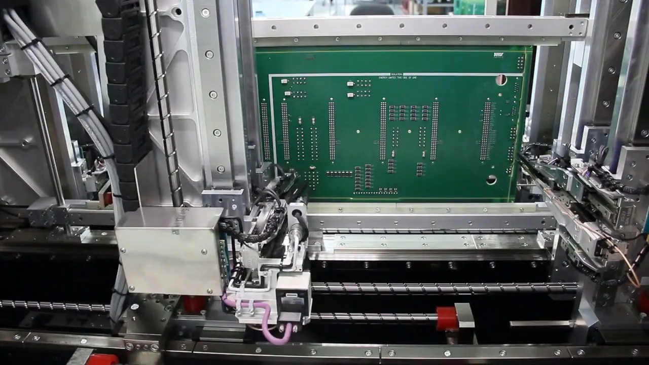
Flying probe testing is an electrical verification method where motorized probes move dynamically across a PCB to test connectivity, isolation, and component values without a custom fixture. Unlike traditional In-Circuit Test (ICT) systems that require a dedicated "bed of nails" fixture, flying probe systems use software-driven movement to access test points on any board design. This flexibility makes it the preferred choice for prototypes, low-volume production runs, and high-mix environments where the cost and lead time of a custom fixture would be prohibitive.
The process works by loading the board's netlist and Gerber data into the testing software, which then calculates the optimal path for the probes to touch every required node. The system checks for shorts (unintended connections), opens (missing connections), and can often measure capacitance and resistance to verify component presence and values. While the test cycle time per board is generally longer than ICT, the elimination of fixture costs and the ability to test complex, high-density boards without physical constraints make it a critical tool for ensuring quality and reliability in modern electronics manufacturing.
The Mechanics of Electrical Verification
Understanding how flying probe systems operate requires a look at the intersection of mechanical precision and electrical logic. At its core, a flying probe tester consists of a gantry system that moves two to four probes independently across the surface of the PCB. These probes are spring-loaded to ensure consistent contact force, typically ranging from 100 to 300 grams, which is sufficient to penetrate the oxide layer on the test pads without damaging the copper or the solder mask.
The testing sequence begins with a calibration routine where the system identifies fiducial markers on the board to establish a precise coordinate system. Once aligned, the software executes a test plan derived from the Design for Test (DFT) data. The probes move to the first test point, make contact, and perform a series of electrical checks. These checks usually include resistance measurements to detect opens and shorts, and sometimes diode or capacitance checks to verify component polarity and value. After the first point is verified, the probes retract and move to the next coordinate, repeating the process until the entire netlist is validated.
One of the most significant advantages of this mechanical approach is its adaptability. In a traditional ICT setup, the fixture is a rigid plate with pogo pins aligned to specific test points. If a design changes, the fixture must be modified or rebuilt, which can take weeks and cost thousands of dollars. With flying probe testing, a design change only requires an update to the software program. The physical hardware remains the same, and the new test plan can be generated and deployed almost immediately. This agility is crucial for industries like medical devices, aerospace, and automotive, where design iterations are frequent and compliance requirements are stringent.
However, the mechanical nature of the test introduces a trade-off in speed. Because the probes must physically travel from point to point, the test time is directly proportional to the number of test points and the distance between them. A board with thousands of test points could take several minutes to test, whereas an ICT fixture could test the same board in seconds. Therefore, the decision to use flying probe testing often comes down to a calculation of volume versus flexibility. For runs under 500 to 1,000 units, the savings on fixture costs usually outweigh the increased cycle time. For high-volume production, the speed of ICT becomes the dominant factor.
Strategic Applications in Modern EMS Workflows
In the context of Electronic Manufacturing Services (EMS), flying probe testing is not just a fallback option; it is a strategic tool for managing risk and cost across different product lifecycles. At Omini, we often see customers attempting to force ICT onto low-volume projects, only to realize that the non-recurring engineering (NRE) costs for the fixture consume the entire project budget. In these scenarios, flying probe testing provides a viable path to quality assurance without the financial burden.
The technology is particularly effective during the New Product Introduction (NPI) phase. When a new design is being validated, the likelihood of finding errors is high. If a board fails an ICT test, the root cause might be a design flaw, a component issue, or a manufacturing defect. With a custom fixture, a design flaw might render the entire fixture useless, requiring a complete rebuild. With flying probe testing, the test program can be adjusted on the fly to accommodate design changes, allowing engineers to iterate quickly. This rapid feedback loop accelerates the time-to-market, a critical metric for competitive industries.
Furthermore, flying probe testing excels in high-mix, low-volume environments. Many EMS providers, including Omini, serve clients who produce a wide variety of specialized equipment in small batches. In such cases, maintaining a warehouse full of ICT fixtures for every product variant is logistically and financially unsustainable. Flying probe systems act as a universal tester, capable of handling dozens of different board designs with just a software switch. This versatility allows manufacturers to offer flexible production services without inflating overhead costs.
Another critical application is in the testing of complex, high-density boards. As PCB designs shrink and component pitches become finer, the physical space available for test points diminishes. Traditional ICT fixtures struggle to accommodate the small pitch of modern BGAs and QFNs without risking short circuits between adjacent pins. Flying probe systems, with their precise computer-controlled movement, can navigate these tight spaces more effectively, provided there is physical access to the pads. For boards with extremely dense routing, this capability is often the only way to perform a comprehensive electrical test without resorting to expensive boundary scan or specialized fixtures.
Integrating Testing with Inspection and Reliability Standards
Electrical testing is only one piece of the quality puzzle. To ensure true reliability, flying probe testing must be integrated into a broader quality ecosystem that includes Automated Optical Inspection (AOI) and X-ray inspection. While flying probes verify that the electrical connections are correct, they do not visually inspect the solder joints or the physical integrity of the components. This is where the synergy between different testing methods becomes vital.
For instance, a flying probe test might confirm that a resistor is present and has the correct resistance value. However, it cannot detect if the resistor is tombstoned, if the solder joint is cold, or if there is a crack in the component body. This is why AOI is typically performed before electrical testing. AOI cameras scan the board to detect soldering defects, missing components, and polarity errors. If AOI catches a physical defect, the board can be reworked before it ever reaches the flying probe tester, saving time and preventing potential damage to the test probes.
Similarly, X-ray inspection is essential for components hidden from view, such as BGAs and QFNs. While flying probe testing can verify the electrical continuity of the nets connected to a BGA, it cannot see the solder balls underneath. X-ray imaging allows engineers to inspect the quality of the solder joints, detect voids, and identify bridging that electrical testing might miss if the bridge is high-resistance. By combining these technologies, manufacturers create a multi-layered defense against defects, ensuring that both the electrical and physical aspects of the assembly meet the required standards.
When discussing reliability, it is also important to consider the IPC standards that govern these processes. The IPC-9252 standard, for example, outlines the requirements for electrical testing of bare boards, while IPC-A-610 covers the acceptability of electronic assemblies. A robust testing strategy aligns with these standards to ensure that the final product meets industry expectations for quality and durability. For a deeper dive into how these standards influence the selection of testing methods, you can review our guide on AOI and X-Ray Inspection in PCB Assembly.
Moreover, the data generated by flying probe tests contributes to the overall traceability of the product. Each test result is logged, creating a digital record that can be used for root cause analysis if a failure occurs in the field. This traceability is increasingly important in regulated industries where the ability to trace a defect back to a specific batch or process step is mandatory. By integrating test data with manufacturing execution systems (MES), manufacturers can gain real-time insights into yield rates and process stability, allowing for continuous improvement.
Practical Considerations for Design and Production
To maximize the effectiveness of flying probe testing, design engineers must consider testability early in the design phase. While flying probe systems are more flexible than ICT, they still require physical access to test points. If the test pads are too small, too close together, or covered by components, the probes may not be able to make reliable contact. This is where Design for Test (DFT) principles come into play. Ensuring that test points are accessible and clearly defined in the Gerber files is crucial for generating an accurate test program.
The quality of the input data is another critical factor. The flying probe system relies on the netlist and Gerber files to determine where to move the probes. If the netlist does not match the physical layout, the test program will be incorrect, leading to false failures or missed defects. It is essential to verify that the data provided by the designer is clean and up-to-date. At Omini, we often work with clients to review their DFM files to ensure that the test points are optimized for the chosen testing method. This collaborative approach helps prevent delays and ensures that the testing process runs smoothly.
For those dealing with heavy copper PCBs, the testing process presents unique challenges. Heavy copper boards often have thicker traces and larger pads, which can affect the contact resistance and the force required for testing. Additionally, the thermal mass of heavy copper can influence the performance of components during testing. Understanding these nuances is vital for avoiding common pitfalls. For a detailed look at design strategies to mitigate these issues, refer to our article on Common Failures in Heavy Copper PCB and How to Avoid Them in the Design Stage.
When planning a production run, it is also important to consider the lead time implications. While flying probe testing eliminates the fixture lead time, the test program generation and verification still take time. For a new design, it may take a day or two to generate the test program, calibrate the machine, and run a few pilot boards to verify the results. This time should be factored into the overall project schedule. However, compared to the weeks required for a custom fixture, this is a negligible delay that offers significant long-term benefits.
Finally, the choice between flying probe and other testing methods should be driven by the specific requirements of the project. If the product is a high-volume consumer electronic device with a stable design, ICT is likely the better choice due to its speed. If the product is a specialized medical device with a low production volume and frequent updates, flying probe testing offers the necessary flexibility. In many cases, a hybrid approach is used, where flying probe is used for initial validation and low-volume runs, and ICT is introduced once the design is mature and production volumes increase.
For a comprehensive overview of how to select the right testing strategy for your specific needs, including the role of functional testing and traceability, our guide on Circuit Card Assembly Testing: Tips and Best Practice provides valuable insights. Additionally, understanding the broader context of Quality and trust process can help ensure that your testing strategy aligns with all relevant industry standards and customer requirements.
Field Notes on Implementation
In practical manufacturing scenarios, the success of flying probe testing often hinges on the collaboration between the design team and the manufacturing partner. It is not uncommon for a design to pass all simulations but fail electrical testing due to minor layout issues that were not apparent in the schematic. This is why early engagement with your EMS provider is crucial. By involving the manufacturing team during the DFM review, potential testability issues can be identified and resolved before the first board is fabricated.
One common misconception is that flying probe testing is a "set and forget" solution. In reality, it requires ongoing maintenance and calibration to ensure accuracy. Probe tips wear out over time and must be replaced regularly to maintain good contact. The machine itself must be calibrated to ensure that the movement is precise and that the electrical measurements are accurate. Neglecting this maintenance can lead to inconsistent results and false failures, which can disrupt production and damage the reputation of the manufacturer.
Another field note concerns the interpretation of test results. A failure in a flying probe test does not always indicate a defect in the board. It could be a result of a dirty probe tip, a calibration error, or a mismatch in the test program. Therefore, it is essential to have a robust failure analysis process in place. When a board fails, the first step should be to verify the test setup and then re-test the board. If the failure persists, a detailed investigation is needed to determine the root cause. This process is similar to the approach used in Custom PCB Board Manufacturer: How to Ensure Quality and Reliability, where systematic analysis is key to maintaining high standards.
Ultimately, flying probe testing is a powerful tool that bridges the gap between design and production. It offers the flexibility needed for modern electronics manufacturing while providing the rigorous verification required for reliable products. By understanding its capabilities, limitations, and strategic applications, manufacturers can make informed decisions that optimize both cost and quality. As the industry continues to evolve, the role of flying probe testing will likely expand, driven by the increasing complexity of PCB designs and the demand for faster time-to-market. For those looking to stay ahead of the curve, mastering this technology is an essential step in building a robust and reliable manufacturing process.