
Direct Answer
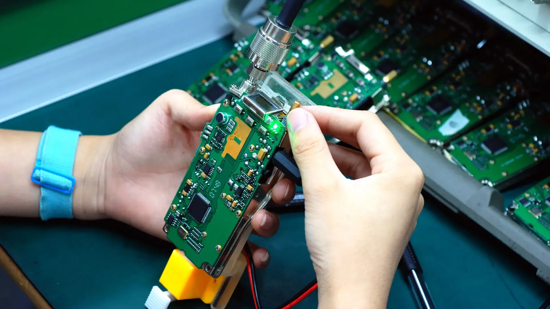
Circuit card assembly testing is the systematic verification that a populated PCB meets electrical, mechanical, and functional requirements before it ships. The most reliable approach combines automated optical inspection (AOI), X-ray analysis, in-circuit test (ICT), and functional test into a layered protocol rather than treating any single method as sufficient. Quality teams that design boards for testability, calibrate fixtures against known-good assemblies, and maintain full component-to-unit traceability catch defects earlier and reduce escaped failures dramatically.
Design for Testability Before the First Component Ships
Testability is not an afterthought bolted onto a finished design. It starts during schematic capture and layout, when engineers decide where test points land, how dense the component population becomes, and whether boundary scan (JTAG) chains are worth the extra routing effort. Boards designed without accessible test points force technicians to probe tiny component leads or vias, increasing measurement error and risk of physical damage.
A practical rule from the production floor: place test points on the bottom side for flying probe or bed-of-nails access, keep them at least 2.54 mm apart to match typical fixture pin spacing, and avoid covering them with large thermal pads or shielding cans. For high-density designs where real estate is scarce, consider dedicated test pads on inner layers accessed via blind vias—costly, but cheaper than a field recall.
Boundary scan deserves particular attention for boards with limited physical access. When processors, FPGAs, and complex ICs include JTAG interfaces, the test engineer can verify interconnects and even program devices without probing individual nets. The upfront cost is additional schematic complexity and slightly larger component BOM. The payoff comes during prototype bring-up and in production, where a single JTAG chain can replace hundreds of physical test points.
Layered Inspection: Why AOI and X-Ray Work Together
No single inspection technology catches every defect. AOI systems excel at detecting missing components, wrong polarity, solder bridging, and insufficient solder on visible joints. Modern machines use multi-angle cameras and machine learning algorithms to classify defect types, but they remain fundamentally surface-level optical—they cannot see what is hidden beneath components or inside solder joints.
This limitation drives the need for X-ray inspection, particularly for area-array packages like BGAs, CSPs, and QFNs where solder connections sit under the device body. X-ray reveals voids, insufficient ball collapse, bridging, and head-in-pillow defects that AOI misses entirely. The combination of both methods, often called AOI and X-Ray Inspection in PCB Assembly, creates a more complete defect detection net than either alone.
In practice, Omini positions AOI after reflow for immediate feedback on the SMT process, then follows with selective X-ray on boards containing hidden solder joints. The AOI data feeds back to the SMT line for real-time parameter adjustment—paste height, placement pressure, reflow profile—while X-ray results target specific component families for deeper process study. This closed-loop approach prevents the same defect from repeating across a production lot.
In-Circuit Test: Catching Manufacturing Defects at Source
ICT remains the workhorse for high-volume production, despite the capital investment in bed-of-nails fixtures. A well-designed ICT program verifies component values, checks for solder opens and shorts, and confirms that polarized devices are oriented correctly—all without ever powering the board fully. This catches the classic manufacturing defects that functional test might miss because the board can still operate marginally with wrong component values or latent solder cracks.
The challenge with ICT is fixture cost and lead time. A dedicated fixture for a complex board can take weeks to fabricate and costs increase with probe count. For low-volume or prototype runs, flying probe testers offer fixtureless flexibility at the expense of longer per-board test time. The decision between bed-of-nails and flying probe often hinges on expected volume, board complexity, and how much design change is anticipated.
Test coverage is another consideration. No ICT achieves 100% coverage on modern dense boards. Some nodes remain physically inaccessible, and certain components like decoupling capacitors in parallel arrays cannot be measured individually. Smart test engineering prioritizes coverage on critical nets—power rails, high-speed signals, safety-related circuits—rather than pursuing perfection that delays production.
Functional Test: Validating the Assembly as a System
Functional test steps back from component-level verification to ask whether the board does what it was designed to do. This requires custom test equipment, software, and often specialized load boards that simulate the end application environment. The investment is significant, but functional test catches integration issues that escape component-level inspection: timing violations, signal integrity degradation, firmware bugs, and thermal performance problems.
A common pitfall is treating functional test as a debugging tool rather than a production gate. When boards fail functional test, the response should be structured failure analysis, not repeated retest until they pass. Omini's approach includes designated debug stations where technicians use the failure signature—power consumption profile, boot sequence behavior, or communication bus activity—to isolate whether the root cause is a manufacturing defect, a design marginality, or a test equipment issue.
Environmental stress during functional test adds another layer of reliability screening. Running boards at temperature extremes, cycling power rapidly, or applying vibration can reveal solder joint fatigue and component infant mortality before products reach customers. The tradeoff is test time and equipment utilization; not every product justifies this level of screening, but medical, automotive, and aerospace applications typically do.
Traceability and Data for Continuous Improvement
Modern quality systems demand more than pass/fail records. Full traceability means linking each assembled board to the specific component lots, solder paste batch, machine placement program, reflow profile, and test results that produced it. When a field failure occurs, this data enables rapid correlation—were all failed boards from the same component reel? Did they share a reflow oven zone profile? Without traceability, failure analysis becomes guesswork.
Implementing traceability starts with barcode or RFID labeling at the bare board stage and extends through every process step. Component feeders on SMT equipment should be loaded from verified lots, with changeover records logged automatically. Test equipment should write results to a central database with board serial numbers, not just maintain local logs that disappear when the machine is repurposed.
The data collected for traceability also drives continuous improvement. Pareto analysis of defect types by machine, by shift, by component supplier, or by board revision reveals patterns invisible at the single-board level. A spike in BGA voiding after a solder paste change, detected through correlated X-ray and traceability data, justifies reverting to the previous paste formulation before customer impact occurs.
Calibration, Golden Boards, and Test Program Validation
Even the best test equipment drifts. Probes wear, camera lighting changes, and measurement thresholds shift with temperature. Regular calibration against known-good assemblies—golden boards with verified electrical characteristics and documented physical condition—prevents false passes and false failures that erode test effectiveness.
A golden board program should include multiple levels: a master golden board stored under controlled conditions, never used for production testing; working golden boards cycled through daily equipment verification; and limit samples deliberately loaded with marginal defects to verify that the test system rejects appropriately. This three-tier structure catches equipment drift before it affects production decisions.
Test program validation deserves equal rigor. When a new product enters production, the test engineer should run the program against golden boards, known-bad boards with specific defects, and a statistical sample from early production. Only after the program demonstrates correct pass/fail discrimination should it be released for production use. Skipping this validation risks shipping boards with undetected defects or scrapping good product due to test error.
Cross-Functional Links to Broader Manufacturing Quality
Circuit card assembly testing does not exist in isolation. The Quality and trust process that governs supplier qualification, material incoming inspection, and process audit schedules creates the foundation on which test effectiveness rests. Similarly, design decisions made early constrain what testing can economically achieve. Rigid-Flex PCB DFM Tips Before PCB Manufacturing illustrates how material selection and bend region design affect both mechanical reliability and the practical challenges of accessing test points on flexible sections.
Component sourcing strategy also intersects with testability. The BOM Risk Strategy for Turnkey PCB Assembly discussion of alternative validation and qualification becomes relevant when substitute components with different electrical characteristics must be tested against original specifications. And for high-speed designs, PCB Stack-Up and Signal Integrity for High-Speed Boards explains how layer construction choices influence whether signal quality tests at functional test represent real-world performance or merely laboratory conditions.
Building a Testing Culture That Catches Problems Early
The most sophisticated test equipment fails when operators treat red flags as nuisances to override. A healthy testing culture empowers technicians to stop the line when trends shift, rewards thorough failure documentation over speed, and invests in training that helps staff distinguish equipment artifacts from real defects. This culture shows up in small practices: the operator who notices a subtle AOI lighting change and requests recalibration; the engineer who spends an extra hour characterizing a marginal failure mode rather than reclassifying it as pass.
Omini has found that the lowest total cost of quality comes not from maximizing test coverage alone, but from aligning test strategy with product risk, customer requirements, and manufacturing volume. A consumer IoT device with six-month market life needs different testing than a pacemaker controller with ten-year expected service. The discipline is making these tradeoffs explicitly, documenting them, and revisiting them when product or market conditions change.
Test strategy is living documentation, not a one-time document filed and forgotten. Each production lot adds data that should refine risk assessment, each field return teaches something about test coverage gaps, and each new component technology demands updated inspection methods. Teams that treat testing as a continuous conversation—between design, manufacturing, quality, and the customer—build products that earn their reliability reputation rather than merely claiming it.