
Direct Answer
The most frequent headaches in SMT circuit board assembly—tombstoning, insufficient solder, component damage, and hidden BGA voids—stem from process variation at the paste-print and pick-and-place stages. Fixing them requires disciplined process control, layered inspection, and design-for-manufacturing feedback rather than relying on downstream rework. In practice, this means validating stencil aperture designs against board finish, calibrating placement force and vision systems for each component family, and closing the loop with real-time SPC data.
Paste Printing: Where Most Defects Begin
Solder paste printing is the highest-leverage step in any SMT assembly line. When print quality drifts, every downstream operation suffers.
Stencil Design and Aperture Control
Aperture area ratios that worked on one PCB assembly job may fail on another due to pad finish, board thickness, or via-in-pad designs. ENIG finishes, for example, present flatter surfaces than HASL, but poor coplanarity between pads can still cause uneven paste deposits. Stencil thickness and aperture wall smoothness determine release efficiency; electropolished or nano-coated stencils reduce clogging on fine-pitch QFNs and 0201 passives. Use the Solder Paste Stencil Calculator to screen area ratio, aspect ratio, and paste volume before stencil release. Omini reviews Gerber and stencil data during DFM to flag area ratios below 0.66 for critical apertures before the first print cycle.
Print Process Monitoring
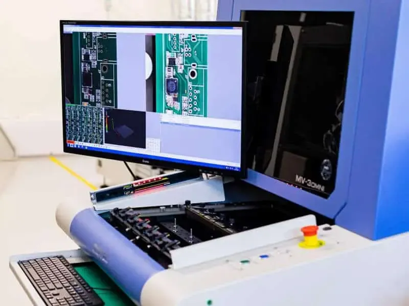
Solder paste inspection (SPI) is not optional for high-mix, medium-volume production. Volume, height, and offset measurements taken after every print catch trends before they become defects. When SPI shows creeping height variation, the root cause is often paste age, humidity exposure, or squeegee pressure drift—not a machine fault. Logging SPI data by job and board revision builds a traceable quality record that pays dividends during customer audits or failure analysis.
Component Placement Accuracy and Feeder Management
Modern pick-and-place machines achieve placement accuracy below 40 µm at 3 sigma, but that specification means little if feeders are loaded with the wrong reel or if component packaging tolerances vary lot-to-lot.
Centroid Data and Programming
Accurate centroid data—the X, Y, and rotation coordinates for each component—prevents placement offsets that manual correction cannot fully fix. When centroid files are extracted from CAD without verification, polarity marks on diodes or orientation-sensitive connectors end up rotated 180 degrees. A quick automated compare against the BOM and Gerber before first article build eliminates these program errors.
Feeder Verification and Changeover Discipline
High-mix environments with frequent changeovers invite reel-loading mistakes. Barcode verification at the feeder level, tied to the shop-floor MES, ensures that the component loaded matches the job pick list. For turnkey assembly jobs where customers consolidate supply, this discipline protects against last-minute substitution errors that can scrap an entire build.
Reflow Profile Optimization and Thermal Management
Reflow is where the solder paste transforms into reliable metallurgical joints. It is also where latent defects from earlier stages become permanent.
Profile Development by Board Mass and Component Density
A single-zone profile cannot serve both a thin IoT sensor board and a heavy server backplane with large BGA thermal mass. Thermocouple placement on representative components—large ground-connected BGAs, small passives, and connectors—reveals delta-T across the assembly. The goal is to maintain all components within the paste manufacturer's recommended time-above-liquidus window while avoiding excessive peak temperature that degrades sensitive packages or rushes cooling that promotes grainy, weaker joints.
Nitrogen Reflow and Oxidation Control
For high-reliability or fine-pitch work, nitrogen atmosphere reflow reduces oxide formation on paste and pad surfaces, improving wetting and reducing voids. The tradeoff is equipment and consumable cost. Deciding when nitrogen is justified depends on the product's end-use environment, not just the component pitch.
Inspection Strategy: Seeing What Matters
No single inspection modality catches every defect mode. A layered approach pays for itself in reduced escapes and warranty returns.
SPI and AOI as Process Controls
Solder paste inspection catches print defects. Automated optical inspection catches placement and solder joint anomalies visible from above. Together, they provide process feedback in near real time. When AOI flags a cluster of shifted components, the fix is often a feeder alignment or nozzle wear issue on the placement machine—not an inspection calibration problem.
X-Ray for Hidden Joints
BGAs, QFNs, and other bottom-terminated components hide their solder joints from optical view. AOI and X-Ray Inspection in PCB Assembly explains how void analysis, ball roundness measurement, and bridging detection under these packages require X-ray penetration. Catching voids above 25% of ball area or misaligned balls before electrical test prevents field failures that functional test alone might miss.
Component Sourcing and BOM Integrity
The most elegant SMT process cannot build a board if parts are unavailable, incorrect, or at risk of obsolescence.
BOM Scrubbing and Alternate Qualification
A BOM handed to manufacturing with vague descriptions or unqualified alternates invites delays. Each line item needs a manufacturer part number, package code, and lifecycle status. For BOM Risk Strategy for Turnkey PCB Assembly, proactive alternate qualification and buffer stock decisions made at the quoting stage prevent mid-build shortages that scramble schedules.
Counterfeit Avoidance
Authorized distribution and incoming inspection of packaging, date codes, and physical characteristics protect against counterfeit components. In turnkey pcba arrangements where the EMS controls procurement, this responsibility sits squarely with the manufacturing partner.
BGA Assembly Specifics
BGA assembly demands tighter process windows than standard SMT due to inaccessible joints and thermal sensitivity.
Pad Design and Via Handling
Via-in-pad designs must be filled and planarized to avoid solder wicking during reflow. Unfilled vias beneath BGAs steal solder from the joint, creating voids or opens. D thermocouples under test BGAs during profile development confirm that the thermal path through the board does not overstress the package.
Rework and Reballing Constraints
BGA rework is expensive and risky. Each thermal cycle degrades the laminate and package. Minimizing rework through upstream process control is far more economical than relying on skilled technicians to salvage marginal boards.
Design for Manufacturing Feedback
Many assembly challenges originate in design decisions made without manufacturing input.
DFM Review Gates
A formal DFM review before PCB fabrication catches component-to-component spacing violations, insufficient keepout around test points, and thermal relief patterns that complicate reflow. Circuit Board Manufacturing Process: A Comprehensive Guide for Beginners walks through how early manufacturing involvement shapes designs that build reliably at volume.
Test Access and Debuggability
Designs that prioritize miniaturization over test access create diagnostic dead ends. Reserved test pads, boundary scan chain completeness, and firmware hooks for in-circuit test reduce debug time when assemblies fail functional verification.
Box Build and System Integration Considerations
For customers requiring box build beyond bare board assembly, SMT quality directly impacts system-level reliability.
Cable and Connector Integration
SMT-mounted connectors with press-fit or cable-attach features require mechanical stability beyond solder joint strength alone. Staking, locking hardware, or bracket reinforcement prevents field failures from vibration or insertion force.
For PLC, remote I/O, motor-control, and connector-heavy builds, use the Industrial Automation PCB Assembly guide to make EMC exposure, enclosure constraints, BOM alternates, and functional-test evidence visible before quote.
ESD and Handling Protocols
Assembled boards are vulnerable to ESD until enclosed in housings. Grounded workstations, ionization, and conductive transport containers maintain protection through final assembly and test.
Closing Field Note
SMT circuit board assembly rewards methodical process control and punishes assumptions. The factories that consistently deliver high-yield, on-time product treat paste printing, placement verification, and layered inspection as interconnected systems—not isolated checkpoints. When design, sourcing, and production teams share data openly, the root causes of defects surface faster and stay fixed longer. PCB assembly capabilities and Circuit Card Assembly Testing: Tips and Best Practice offer additional perspective on building reliability in from the start. For teams pushing into finer pitches, denser layouts, and shorter lead times, the margin for process sloppiness keeps shrinking—and the competitive advantage goes to those who invest in preventing problems rather than reacting to them.