
پاسخ مستقیم
ENIG and OSP surface finish trends directly determine SMT assembly risk through their impact on solder wetting, intermetallic formation, and defect rates such as head-in-pillow and voiding. You evaluate this risk by matching finish properties to your component package types, reflow profile, and reliability requirements, then verifying finish thickness and shelf life in the RFQ before committing to a build.
---
Why Surface Finish Selection Is a Risk Decision, Not a Cost Decision
The surface finish on your PCB pads is the chemical interface between the copper circuitry and the solder paste that forms every SMT joint. It controls how well solder wets, how quickly intermetallic compounds form, and how the joint behaves under thermal and mechanical stress. When finish trends shift—whether due to supply chain pressure, environmental regulations, or cost optimization—the risk profile of your assembly changes even if the rest of your design stays identical.
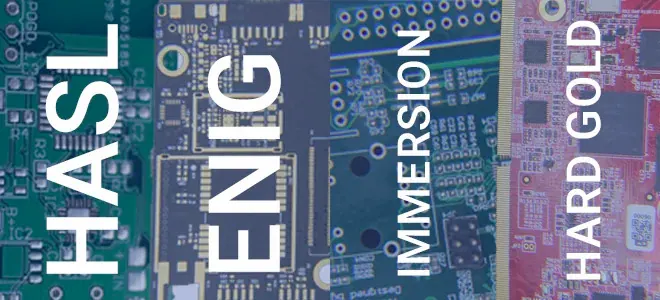
OSP (Organic Solderability Preservative) and ENIG (Electroless Nickel Immersion Gold) represent two fundamentally different approaches to protecting copper. OSP is a thin organic coating that keeps copper clean until reflow. ENIG deposits a nickel barrier layer followed by a thin gold layer to prevent oxidation. Neither is universally superior; each carries specific failure modes that become more or less likely depending on your board design and assembly process.
The practical question is not "which finish is better" but "which finish is better for this specific board, this component mix, and this reliability target." Evaluating that requires looking at finish trends through the lens of wetting behavior, intermetallic formation, package compatibility, and inspection capability.
---
How ENIG and OSP Trends Affect Solder Wetting and Intermetallic Formation
Solder Wetting Behavior
Solder wetting is the first physical event that determines joint quality. When molten solder contacts a pad, it must spread, wet the surface, and form a continuous metallurgical bond. The surface finish directly controls this behavior.
OSP-coated copper provides an excellent wetting surface as long as the coating is intact and the board is assembled within its shelf life. The organic layer volatilizes during reflow, exposing clean copper to the molten solder. The resulting copper-tin intermetallic is well understood and reliable. The risk appears when the OSP layer degrades—through multiple reflow cycles, prolonged storage, or improper handling—leaving oxidized copper that solder will not wet.
ENIG provides a flat, oxidation-resistant surface that wets consistently even after extended storage. The gold layer dissolves into the solder during reflow, exposing the nickel layer, which forms a nickel-tin intermetallic. This intermetallic is more brittle than copper-tin but also more stable at elevated temperatures. The wetting risk with ENIG is not oxidation but the "black pad" phenomenon, where corrosion of the nickel layer during the immersion gold process creates a weak, non-wetting surface.
Intermetallic Formation and Joint Reliability
The intermetallic compound (IMC) layer is the metallurgical bond between the solder and the pad. Its thickness and morphology determine joint strength and long-term reliability.
With OSP, the copper-tin IMC grows quickly during reflow and continues to grow slowly during thermal aging. Excessively thick IMC layers become brittle and prone to fracture under thermal cycling or mechanical shock. This matters more for boards that will experience high operating temperatures or many power cycles.
With ENIG, the nickel-tin IMC grows more slowly, which is an advantage for high-temperature applications. However, the nickel layer thickness and phosphorus content in the electroless nickel must be controlled. If the nickel is too thin or has excessive phosphorus, the IMC can become irregular and weak. The gold layer thickness also matters: if the gold is too thick, it can create gold-embrittlement in the solder joint, though this is rare with typical immersion gold thicknesses.
Practical Assessment Approach
For a given board, evaluate wetting and IMC risk by considering:
- Component density: Fine-pitch components and BGAs require consistent wetting across all pads. ENIG's flatness and oxidation resistance reduce wetting variability.
- Reflow profile: Higher peak temperatures and longer time above liquidus accelerate IMC growth. Match the finish to your profile's thermal exposure.
- Operating environment: High-temperature or high-vibration applications favor the slower-growing nickel-tin IMC of ENIG.
- Board thickness and copper weight: Thicker copper requires more heat to reach reflow temperature, which can stress OSP coatings near their decomposition point.
---
Matching Surface Finish to Component Package Types
BGA and Fine-Pitch Components
BGA assembly is where finish selection has the most visible impact on yield. The solder balls on a BGA must collapse, wet, and form a consistent joint across the entire array. Any variation in pad wetting translates directly into head-in-pillow defects or non-wetting.
ENIG's flat, uniform surface is the safer choice for BGAs with pitch below 0.8 mm. The nickel barrier prevents copper dissolution into the solder ball, which can cause pad cratering or "solder ball collapse" issues. The flat surface also improves coplanarity, which matters when the BGA package itself has slight warpage.
OSP can work for BGAs with pitch above 0.8 mm, but the risk increases with finer pitch. The organic coating must be uniform across all pads, and the board must be assembled promptly after fabrication. If the OSP thickness varies—thicker in the board center, thinner at the edges—wetting will vary across the BGA array, creating intermittent opens that are difficult to detect without X-ray.
Passive Components and Standard ICs
For 0402 and larger passives, and for QFP or SOP packages, both finishes perform well. The primary risk with OSP is handling-related: fingerprints, moisture, or contamination on the pads before reflow. The primary risk with ENIG is cost and the low but nonzero black pad risk.
For these components, the decision often comes down to logistics rather than technical performance. If your board will sit in inventory before assembly, ENIG's longer shelf life reduces risk. If you are assembling within weeks of board fabrication, OSP is technically sufficient and lower cost.
Mixed-Technology Boards
Boards with both SMT and through-hole components introduce another variable. If the board requires selective soldering or wave soldering after reflow, the finish must survive both processes. OSP degrades with each thermal excursion; a second pass through a wave solder pot can strip the coating from through-hole pads, leaving them oxidized before solder contact. ENIG handles multiple thermal excursions without degradation.
If your board has a mix of fine-pitch BGAs and through-hole connectors, you may need to choose ENIG to protect the BGA side while accepting the cost premium. Alternatively, you can use OSP and adjust the process to minimize thermal exposure on the second side.
---
Evaluating Finish Thickness and Shelf Life in the RFQ
What to Specify in the RFQ
The RFQ is where finish risk is either controlled or ignored. A vague statement like "ENIG finish" or "OSP per IPC" leaves too much room for interpretation. Your RFQ should include:
- Finish type: Explicitly state ENIG or OSP, not "any solderable finish."
- Thickness range: Specify the acceptable range for the finish. For ENIG, this includes both nickel and gold thickness. For OSP, specify the coating thickness range.
- Shelf life requirement: State the maximum allowable time between board fabrication and assembly, and require the manufacturer to date-code the boards.
- Reflow compatibility: Note the number of reflow cycles the finish must survive.
- Inspection requirements: Specify whether you will perform X-ray, AOI, or cross-sectioning on first articles.
How to Verify Finish Compliance
Before the build, request the board fabricator's finish certification. This should include thickness measurements taken from the actual production panels, not just a certificate of conformance. For ENIG, verify both nickel and gold thickness. For OSP, verify coating thickness and uniformity.
If you are working with an EMS provider, ask them to perform incoming inspection on the bare boards. A simple visual check for OSP color uniformity—it should be a consistent light gold to amber—can catch coating problems. For ENIG, a visual check for discoloration or pitting can catch black pad issues before assembly.
Shelf Life and Storage Conditions
OSP has a practical shelf life of 6 to 12 months from fabrication, depending on storage conditions. Humidity and temperature accelerate oxidation. If boards are stored in a humid environment, the OSP can degrade in weeks. ENIG has a shelf life of 12 months or more, and is more forgiving of storage conditions.
The risk with OSP shelf life is not that the board looks bad—it can look fine while the coating has degraded to the point where wetting fails. The risk with ENIG is more subtle: the nickel layer can become passive over time, reducing wetting even though the gold layer looks intact.
> Practical note: If your board has been in storage for more than three months, run a small test batch before committing to full production. Solder a few boards and inspect the joints under X-ray. This catches finish degradation before it becomes a yield problem.
---
Inspection Methods for Finish-Related Defects
X-Ray Inspection for BGA Voiding and Head-in-Pillow
X-ray inspection is the primary tool for detecting finish-related BGA defects. Voiding in BGA solder joints can be caused by outgassing from the OSP coating or from moisture absorbed by the board. ENIG reduces voiding risk because the nickel barrier prevents copper from dissolving into the solder, which can create gas bubbles.
When evaluating X-ray images, look for:
- Void distribution: Voids clustered near the pad interface suggest a finish or flux issue. Voids distributed throughout the joint are more likely from solder paste or reflow profile issues.
- Head-in-pillow: This appears as a visible separation between the solder ball and the pad solder. It indicates that the ball reflowed but did not wet the pad, often due to finish oxidation or warpage.
- Non-wetting: Pads that show no solder attachment at all, visible as bright areas in the X-ray image.
AOI for Wetting and Solder Joint Appearance
Automated optical inspection (AOI) catches finish-related issues on visible joints. Poor wetting appears as a dull, grainy solder surface or as solder that does not wet up the component lead. For OSP boards, look for pads that appear darker or discolored after reflow—this indicates the coating did not fully volatilize.
AOI is less useful for BGA joints, which are hidden under the package. For those, X-ray is required. Use AOI for visible components and X-ray for BGAs, and correlate the results. If AOI shows wetting issues on visible pads, the hidden BGA joints likely have similar problems.
بازرسی ماده اول
The first-article inspection is your best opportunity to catch finish-related issues before committing to full production. On the first article, perform:
- Cross-sectioning on representative BGA joints to measure IMC thickness and check for voids.
- Shear testing on a few components to verify joint strength.
- X-ray on all BGA packages to establish a baseline for voiding.
Compare the results against your reliability requirements. If IMC thickness is excessive or voiding is above your threshold, investigate the finish before continuing.
---
Common Mistakes in ENIG and OSP Selection
Assuming OSP Is Always Cheaper
OSP is cheaper per square foot than ENIG, but the total cost includes yield loss, rework, and field failures. If OSP causes a 2% yield loss on a board with expensive components, the cost advantage disappears. Calculate the total cost of ownership, not just the finish cost.
Ignoring the Impact of Multiple Reflow Cycles
Boards that go through reflow more than once—for double-sided assembly or for rework—stress the finish differently. OSP degrades with each thermal cycle. If your board requires two reflow passes, the second side may have marginal wetting. ENIG handles multiple passes without degradation.
Not Checking the Nickel Thickness in ENIG
The gold layer is what you see, but the nickel layer is what determines reliability. Thin nickel allows copper to diffuse through to the surface, creating a weak intermetallic. Always verify nickel thickness in the RFQ and on the certification.
Assuming ENIG Eliminates All Defects
ENIG reduces but does not eliminate assembly risk. Black pad, gold embrittlement, and nickel passivation are all possible. ENIG boards still require proper reflow profiles and inspection.
Overlooking the Board Design Interaction
The finish does not exist in isolation. Pad size, solder mask opening, and copper weight all interact with the finish. A board with oversized pads and OSP finish may have solder wicking issues. A board with fine-pitch pads and ENIG may have solder mask alignment issues that expose copper. Review the finish in the context of your land pattern design, referencing IPC-7351 for footprint dimensions and tolerances.
---
مثال عملی: ارزیابی هیئت فناوری ترکیبی
Consider a control board with the following characteristics:
- Stackup: 6-layer, 1.6 mm total thickness, FR-4 with 1 oz copper on outer layers
- Components: One 0.5 mm pitch BGA, several QFPs, 0402 passives, and two through-hole connectors
- Assembly: Double-sided SMT with selective soldering for the through-hole connectors
- Reliability requirement: 10-year service life in an industrial environment with moderate temperature cycling
Risk evaluation for OSP:
- The 0.5 mm pitch BGA is a concern. OSP can work, but wetting variability across the BGA array increases the risk of head-in-pillow.
- The selective soldering step will expose the OSP to a second thermal excursion, potentially degrading the coating on the through-hole pads.
- Shelf life is manageable if the boards are assembled within three months of fabrication.
Risk evaluation for ENIG:
- The BGA is well-served by ENIG's flat, uniform surface.
- The selective soldering step will not degrade the ENIG finish.
- Cost is higher, but the yield risk is lower.
Recommendation: ENIG for this board. The BGA pitch and the selective soldering step create enough risk that the OSP cost savings are not justified. If the BGA were removed or the pitch increased to 0.8 mm, OSP would be a reasonable choice.
---
How to Involve Your EMS Partner Early
Finish selection is not a decision to make in isolation. Your EMS partner sees the assembly results across many boards and can provide practical guidance on finish performance with your specific component mix and reflow equipment.
Involve the EMS partner during design review, not after the boards are fabricated. Provide them with:
- The board stackup and copper weight
- The component list with package types
- The planned reflow profile
- The reliability test requirements
Ask them to review the finish selection against their process capability. They may have data on how OSP performs with their specific reflow oven or how ENIG behaves with your solder paste formulation.
The EMS partner should also be involved in the first-article inspection. Their X-ray and AOI equipment will be used to evaluate the finish, so they need to know what defects to look for. If you have specific reliability tests planned—thermal cycling, drop testing, or vibration—communicate those early so the finish can be evaluated against them.
For related risk evaluations, review how board design and layout choices interact with finish selection, and how FOPLP and thermal processing trends affect reflow requirements. Environmental and regulatory trends also influence finish availability, as covered in the analysis of CEO and REACH trends and CEO and yield trends. Sourcing trends in PCB fabrication can also affect finish consistency across suppliers.
---
پرسشهای متداول
Why do ENIG and OSP trends matter for SMT assembly risk?
ENIG and OSP trends matter because the surface finish directly controls solder wetting, intermetallic formation, and the risk of defects like head-in-pillow or voiding during SMT assembly. Choosing the wrong finish for your board design and component mix can lower yield and field reliability, so you need to evaluate the finish against your specific assembly process and reliability requirements.
Where do engineers make the biggest mistakes when choosing between ENIG and OSP?
Engineers often assume OSP is always cheaper and ENIG is always more reliable, or they ignore the impact of the finish on BGA assembly and reflow. Another common mistake is not checking the OSP thickness or the ENIG nickel thickness against the supplier's specification, which can cause wetting or solder joint embrittlement issues.
How can I verify ENIG or OSP suitability before the build?
Before build, review the finish specification against your BOM and board design. For OSP, verify the coating thickness and ensure the board is assembled within the OSP's shelf life. For ENIG, check the nickel and gold thickness, and confirm the finish is compatible with your reflow profile and any selective soldering steps.
What information should I provide in the RFQ to evaluate ENIG and OSP risk?
In the RFQ, include the required surface finish, the finish thickness range, the board stackup, the component list with package types, and the reflow profile you plan to use. Also state any reliability tests you need, such as thermal cycling or drop testing, so the manufacturer can assess the finish's impact on your specific assembly.
What are the key trade-offs between ENIG and OSP for SMT assembly?
ENIG provides a flat, oxidation-resistant surface that is ideal for fine-pitch and BGA assembly, but it costs more and can have black pad risks. OSP is cheaper and works well for most SMT assemblies, but it has a shorter shelf life and requires careful handling to avoid oxidation before reflow.
> Engineering handoff note: How to Evaluate SMT Assembly Risk from FOPLP and Thermal Processing Trends, How to Evaluate SMT Assembly Risk from Board Design and Board Layout, and How to Evaluate SMT Assembly Risk from CEO and REACH Trends before the release package is frozen.
> Also compare How to Evaluate SMT Assembly Risk from CEO and Yield Trends and How to Evaluate SMT Assembly Risk from PCB Fabrication and Sourcing Trends before locking the quote scope.
> Engineering handoff note: How to Evaluate SMT Assembly Risk from Supply Chain and Lead Time Trends before the release package is frozen.