
Direct Answer
Evaluate SMT assembly risk from MCU and industrial trends by comparing package-specific process demands against your PCBA partner's stencil, reflow, and inspection capabilities during DFM review. Shrinking MCU packages like 0.4 mm QFN and 0.5 mm BGA require tighter paste volume control, while industrial automation end-use raises reliability expectations for solder joint integrity. A structured risk assessment covering package data, board stackup, and inspection planning prevents costly rework and field failures.
Why MCU Package Evolution Changes the Risk Equation
MCU package trends are not just a sourcing concern; they directly alter the physical constraints of your SMT assembly process. As MCUs migrate from traditional QFP packages to QFN, dual-row QFN, and fine-pitch BGA, the assembly risk profile shifts in three specific areas: solder paste deposition, component placement accuracy, and reflow profile control.
The Transition from QFP to QFN and BGA
Traditional QFP packages with 0.5 mm or 0.65 mm pitch have exposed leads that are relatively forgiving during reflow. The leads provide visible solder fillets that are easy to inspect with AOI. QFN packages, by contrast, have hidden terminations under the component body. A 0.4 mm pitch QFN requires stencil apertures that are typically 0.2 mm wide or narrower, which reduces the paste volume available for each joint. This increases the risk of opens, especially if the stencil design does not account for the specific pad geometry.
BGA packages add another layer of complexity. A 0.5 mm pitch BGA on an MCU demands a solder ball diameter around 0.3 mm, and the resulting standoff height after reflow is only about 0.2 mm. This tight geometry leaves little room for error in paste volume, placement accuracy, or board flatness. If your PCB has a thickness of 1.6 mm with a 4-layer stackup, the coefficient of thermal expansion mismatch between the board and the BGA package becomes a reliability consideration that a 2-layer board would not present.
Dual-Row QFN: A Specific Risk Case
Dual-row QFN packages are increasingly common in industrial MCUs because they offer more I/O in a compact footprint. However, they present a specific stencil design challenge. The inner row of pads is typically narrower than the outer row, and the paste release from the stencil is less efficient for the smaller apertures. If your assembler uses a single stencil thickness for both rows, you risk insufficient solder on the inner row or solder bridging on the outer row.
A practical approach is to request a step stencil or a custom aperture design that accounts for the area ratio of each pad row. The IPC-7525 stencil design guideline recommends an area ratio above 0.66 for reliable paste release. For a dual-row QFN with 0.4 mm pitch, the inner row apertures may fall below this threshold, requiring a laser-cut stencil with electropolishing to improve release.
> Rule of thumb: If your MCU package has a pitch below 0.5 mm, request a stencil design review before committing to tooling. The stencil is the cheapest component in your assembly; rework is the most expensive.
Industrial Automation Trends and Their Impact on Assembly Requirements
Industrial automation trends push MCU-based PCBA designs toward higher reliability expectations than consumer electronics. These products operate in environments with vibration, temperature cycling, and potential exposure to contaminants. The SMT assembly process must produce solder joints that survive these conditions, which changes how you evaluate assembly risk.
Vibration and Thermal Cycling Demands
Industrial automation controllers, motor drives, and sensor interfaces often experience continuous vibration. This places mechanical stress on solder joints, particularly for larger MCU packages like QFN and BGA. A QFN package with a large exposed pad relies on the solder joint under the pad for both thermal and mechanical connection. If the solder paste volume is insufficient, voids can form, reducing the effective attachment area and increasing the risk of crack propagation under vibration.
Thermal cycling is another concern. Industrial environments may see temperature swings from -20°C to 85°C or wider. The CTE mismatch between a 0.4 mm pitch QFN package and an FR-4 board with 1 oz copper can cause shear stress on the solder joints. Your reflow profile must ensure complete wetting and proper intermetallic compound formation. A profile with a peak temperature too low or a time above liquidus too short will produce weak joints that fail prematurely in the field.
Inspection Requirements for Higher Reliability
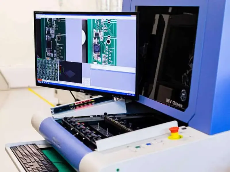
Industrial automation end-use raises the bar for inspection. While a consumer product might pass with AOI alone, an industrial MCU board often requires X-ray inspection for BGA and QFN packages. X-ray is the only practical method to verify solder joint integrity under a BGA or QFN body. It can detect voids, bridging, and insufficient solder that AOI cannot see.
Your risk assessment should include a clear inspection plan. For a QFN with a large exposed pad, X-ray can verify that the pad is at least 75% covered with solder, though the exact acceptance criteria should follow your internal quality standards or IPC-A-610 scope for assembled board acceptability. For BGA, X-ray can detect head-in-pillow defects, which are particularly problematic in lead-free assemblies with certain surface finishes.
The cost of X-ray inspection is justified when the MCU is the primary processing element in an industrial control system. A field failure of that MCU board could mean production downtime, which far exceeds the incremental inspection cost.
Evaluating Risk During Design Review and BOM Validation
The most effective time to evaluate SMT assembly risk is before you commit to tooling and stencil fabrication. A structured design review should cover package data, board stackup, and the interaction between the two.
Package Data and Land Pattern Verification
Start by verifying the MCU package dimensions against the land pattern in your PCB design. Use IPC-7351 as the reference for land pattern dimensions. A common mistake is using the manufacturer's recommended land pattern without checking whether it is compatible with your board stackup and assembly process.
For example, a 0.5 mm pitch BGA with a 0.3 mm solder ball requires a land pad diameter around 0.25 mm. If your PCB fabrication process produces pads with a tolerance of ±0.05 mm, the actual pad size may vary from 0.20 mm to 0.30 mm. This variation directly affects the solder joint shape and reliability. Your design review should account for these tolerances.
Moisture Sensitivity Level and Handling
MCU packages are classified by moisture sensitivity level per J-STD-020. A QFN or BGA with MSL 3 or higher must be baked before assembly if it has been exposed to ambient humidity for more than the allowable floor life. This is a risk factor that often gets overlooked during BOM validation.
If your MCU is MSL 3 and your assembler does not have proper dry storage, you risk "popcorning" during reflow. The trapped moisture expands rapidly, causing internal delamination or package cracking. This defect is not always visible externally and may only manifest as intermittent electrical failures in the field.
Your BOM should include the MSL rating for each MCU, and your RFQ should specify the required handling procedures per J-STD-033. Ask your assembler about their dry storage capacity and whether they can accommodate MSL 2 or MSL 3 parts without extended lead times.
Centroid File Accuracy as a Risk Multiplier
The centroid file is the data that drives your pick-and-place machine. If the centroid data is inaccurate, the MCU will be placed off-center, causing tombstoning, bridging, or opens. This risk increases with finer pitch packages.
A common source of error is using the centroid data from the schematic symbol rather than the PCB footprint. The two may differ if the footprint has been modified for thermal relief or test points. Your design review should include a cross-check of the centroid file against the Gerber data.
When MCU supply shifts force an alternate package or footprint change, the centroid file must be regenerated and re-verified. This is a risk multiplier because the change may affect not only placement but also stencil apertures and reflow profile. A thorough BOM validation should flag any MCU alternates that have different package types.
Practical Risk Assessment Framework for Turnkey PCBA Planning
A structured framework helps you evaluate assembly risk consistently across different MCU choices and board designs. The following table summarizes the key risk factors and the data you need to assess them.
| Risk Factor | Data Required | Assessment Question |
|---|---|---|
| Package pitch | Package datasheet, land pattern | Is the pitch below 0.5 mm, requiring special stencil design? |
| Solder paste volume | Stencil aperture design, area ratio | Does the aperture area ratio exceed 0.66 for all pads? |
| Reflow profile | Package MSL, solder paste datasheet | Does the profile meet the paste manufacturer's recommendations? |
| Inspection capability | X-ray, AOI, first-article plan | Can the assembler inspect hidden joints under QFN/BGA? |
| Board stackup | Layer count, copper weight, thickness | Does the stackup minimize CTE mismatch with the MCU package? |
| BOM alternates | Alternate part numbers, package types | Do alternates have the same package and assembly requirements? |
First-Article Inspection as a Risk Mitigation Tool
First-article inspection is the most direct way to verify that your assembly process can handle the MCU package. The first-article should include X-ray inspection for any BGA or QFN package, cross-sectioning if required by your reliability specification, and electrical test.
Your first-article plan should specify the acceptance criteria before the build starts. For a QFN, this might include a maximum void percentage under the exposed pad. For a BGA, it might include a minimum solder ball diameter after reflow. These criteria should be based on your product requirements, not just the assembler's standard practice.
When to Involve Your PCBA Partner
Involve your PCBA partner early, ideally during the design review phase. A partner like Omini can provide feedback on stencil design, reflow profiling, and inspection planning before you commit to tooling. This is particularly important when you are using a new MCU package or transitioning from a QFP to a QFN or BGA.
The cost of a DFM review is small compared to the cost of rework or field failures. A DFM review should cover pad design, solder mask openings, thermal relief, and test point accessibility. For MCU boards, test point accessibility is critical because the fine pitch of the MCU makes it difficult to probe directly.
Common Mistakes and How to Avoid Them
Engineers often make predictable mistakes when evaluating SMT assembly risk from MCU and industrial trends. Recognizing these patterns helps you avoid them.
Focusing Only on Component Availability
The most common mistake is treating MCU risk as purely a supply chain issue. Engineers spend significant effort on lead time and alternate sourcing but ignore the assembly implications of a package change. A dual-row QFN alternate to a QFP original is not a drop-in replacement from an assembly perspective. The stencil, reflow profile, and inspection plan all need to change.
Assuming a Universal Reflow Profile
Another mistake is assuming the same reflow profile works for all MCUs. A 0.4 mm pitch QFN with a large exposed pad may require a different soak time than a 0.8 mm pitch QFP. The solder paste manufacturer's datasheet provides a recommended profile, but the actual profile must be tuned for the specific board mass and component density. A profile that works for a simple 2-layer board may not work for a dense 8-layer industrial controller board.
Overlooking Board Stackup Effects
The board stackup affects assembly risk in ways that are not always obvious. A thicker board, such as 2.0 mm, has more thermal mass and requires more heat during reflow. This can cause temperature differences across the board, leading to poor wetting on some joints. A board with mixed copper weights, such as 1 oz on outer layers and 2 oz on inner layers, also has different thermal characteristics.
Ignoring Inspection Limitations
Finally, engineers sometimes specify inspection requirements that the assembler cannot meet. For example, if your MCU is a 0.4 mm pitch BGA, you need X-ray with sufficient resolution to detect solder ball defects. Not all X-ray systems can handle this. Your RFQ should specify the inspection requirements and ask the assembler to confirm their capability.
For related risk factors, review how How to Evaluate SMT Assembly Risk from FOPLP and Thermal Processing Trends applies to advanced packaging, and consider How to Evaluate SMT Assembly Risk from Aerospace and Industrial Automation Trends for higher-reliability environments.
What to Include in Your RFQ to Reduce Assembly Risk
A well-structured RFQ reduces assembly risk by giving your PCBA partner the information they need to assess manufacturability. The following items should be included.
Required Documentation
Provide the full BOM with manufacturer part numbers, package types, and MSL ratings. Include the centroid file in the correct format, typically CSV or Excel, with columns for reference designator, X position, Y position, rotation, and layer. Provide the Gerber files and the PCB stackup details, including layer count, copper weight, and dielectric thickness.
Process and Reliability Requirements
Specify any reliability requirements, such as X-ray inspection for BGA or QFN, conformal coating for harsh environments, or specific reflow profile requirements. If you have a preferred reflow profile from your solder paste manufacturer, share it. If not, ask the assembler to recommend one based on the BOM and board stackup.
Questions to Ask Your Assembler
Ask about their experience with the specific MCU package you are using. Have they assembled 0.4 mm pitch QFN packages before? What is their X-ray inspection capability? Do they have dry storage for MSL-sensitive components? What is their first-article inspection process?
For additional context on how market and leadership changes affect assembly risk, see How to Evaluate SMT Assembly Risk from Acquisition and CEO Trends. For automotive-specific considerations, review How to Evaluate SMT Assembly Risk from Automotive and ADAS Trends. And for broader design and fabrication factors, see How to Evaluate SMT Assembly Risk from PCB Design and PCB Manufacturing Trends.
Frequently Asked Questions
Why do MCU trends matter for SMT assembly risk?
MCU packages are shrinking and using finer pitches, such as 0.4 mm QFN and 0.5 mm BGA. These packages demand tighter stencil apertures, precise solder paste volume, and controlled reflow profiles. If your PCBA partner lacks experience with these packages, you risk opens, shorts, and reliability failures.
Where do engineers make mistakes when assessing SMT assembly risk from MCU trends?
A common mistake is focusing only on component availability and ignoring package-specific assembly requirements. For example, a dual-row QFN may need a specific stencil design to avoid solder bridging. Another mistake is assuming the same reflow profile works for all MCUs, which can cause voiding or poor wetting.
How can I verify SMT assembly risk before building my PCBA?
Review the MCU package dimensions, land pattern per IPC-7351, and moisture sensitivity level per J-STD-020. Provide your assembler with the BOM, centroid file, and Gerber data for a DFM review. Ask about their experience with similar packages and request a first-article inspection plan.
What information belongs in the RFQ to reduce SMT assembly risk?
Include the full BOM with manufacturer part numbers, package types, and moisture sensitivity levels. Provide the centroid file and PCB stackup details. Specify any reliability requirements, such as X-ray inspection for BGA or QFN, and share your reflow profile if you have one.
How do industrial automation trends affect SMT assembly risk?
Industrial automation products often run in harsh environments with high vibration and temperature swings. This increases the need for robust solder joints, conformal coating, and thorough inspection. Your PCBA partner must be able to handle these reliability demands, not just place components.
What is the role of a DFM review in reducing MCU assembly risk?
A DFM review catches package-specific issues before tooling and stencil commitments. It verifies that the land pattern matches the package, the stencil apertures are appropriate for the pitch, and the inspection plan covers hidden joints. A DFM review with a manufacturing partner like Omini is a low-cost way to avoid high-cost rework.