
Direct Answer
Evaluate SMT assembly risk from BGA trends by comparing package pitch, ball diameter, and MSL against your board stackup, surface finish, and reflow capability before quoting. Fine-pitch BGAs below 0.8 mm pitch increase stencil, coplanarity, and inspection risk. Check warpage limits, plan X-ray coverage, and send complete RFQ data so your assembler can flag issues early.
Why BGA Package Trends Are Changing the Risk Profile
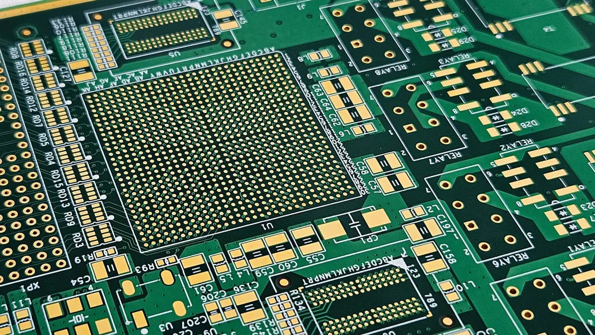
BGA packages have moved from 1.27 mm pitch to 0.8 mm, 0.65 mm, and even 0.4 mm pitch in high-density designs. At the same time, body sizes have grown to accommodate more I/O, and some packages now exceed 40 mm on a side. These two trends—finer pitch and larger body—create opposing mechanical stresses during reflow.
A 0.4 mm pitch BGA has solder balls with a diameter of roughly 0.25 mm. That leaves very little solder volume to form a reliable joint. The stencil aperture for such a package must be smaller than the pad, which reduces paste volume further. If the board surface finish is uneven or the solder mask registration is off, you lose margin that a 1.27 mm pitch package would absorb without issue.
Larger body sizes also increase the risk of package warpage. A 35 mm BGA can exhibit dynamic warpage during reflow that exceeds the coplanarity specification, especially if the mold compound and substrate have mismatched coefficients of thermal expansion. When the package warps at peak reflow temperature, the corner balls may lift away from the paste, creating head-in-pillow defects that are difficult to detect without X-ray.
The practical result is that BGA assembly risk is no longer just about placement accuracy. It now depends on the interaction between package construction, board design, stencil design, and reflow profile. Evaluating these factors before you commit to a PCBA build is the only way to avoid costly rework or field failures.
Package-Level Risk Factors to Review First
Pitch, Ball Diameter, and Land Pattern Design
The first step in evaluating BGA assembly risk is to read the package datasheet and extract three numbers: pitch, ball diameter, and ball count. These determine the land pattern, stencil aperture, and inspection requirements.
For pitches above 0.8 mm, standard stencil design rules generally work. For 0.8 mm pitch, you need to pay attention to aperture area ratio. For 0.65 mm and below, you should consider electroformed stencils or laser-cut stencils with electropolishing to improve paste release. The area ratio—the aperture opening area divided by the aperture wall area—should stay above 0.66 for good paste transfer. At 0.4 mm pitch, achieving that ratio requires a stencil thickness of 0.1 mm or less, which reduces paste volume for other components on the board.
The land pattern itself should follow IPC-7351 recommendations for the specific package type. A common mistake is using the same pad size for a 0.5 mm pitch BGA as for a 0.8 mm pitch BGA. The smaller pitch requires smaller pads to prevent solder bridging, but smaller pads also mean less solder joint standoff height, which reduces reliability under thermal cycling.
Coplanarity and Warpage Specifications
Coplanarity is the deviation of the solder ball tips from a single plane. J-STD-020 defines the moisture sensitivity level and reflow classification, but coplanarity is typically specified in the package datasheet. Most BGAs specify a coplanarity limit of 0.1 mm or less. If your board has significant warpage, the combined package and board warpage can exceed this limit during reflow.
Dynamic warpage is harder to evaluate because it changes with temperature. Some package suppliers provide warpage data at different temperatures, but many do not. If you are using a new or unfamiliar BGA, ask the supplier for warpage data at 25°C, 217°C, and 260°C. If that data is not available, plan for a first-article build with X-ray inspection to verify joint quality.
> Practical note: If your board is thicker than 1.6 mm or has uneven copper distribution, ask your assembler to check board warpage at reflow temperatures. A board that is flat at room temperature can bow significantly at 245°C, especially with mixed-layer stackups.
Moisture Sensitivity Level and Bake Requirements
BGAs are among the most moisture-sensitive components in SMT assembly. J-STD-020 assigns an MSL rating that determines the floor life after the moisture barrier bag is opened. J-STD-033 provides handling, packing, and baking requirements.
A common mistake is assuming that all BGAs are MSL 3. Many fine-pitch and large-body BGAs are MSL 4 or MSL 5, which means they absorb moisture faster and require baking if exposed to ambient humidity for more than a few hours. If a moisture-sensitive BGA is reflowed without proper baking, the trapped moisture can vaporize and cause "popcorning"—internal delamination that is not visible from the outside but can cause intermittent opens or shorts.
Before the build, verify the MSL rating for every BGA in your BOM. If any component is MSL 4 or higher, confirm that your assembler has the baking capability and that the schedule accounts for bake time. Baking is typically done at 125°C for 24 to 48 hours, which can add days to the lead time if not planned.
Board-Level Risk Factors That Affect BGA Reliability
Stackup, Copper Balance, and Surface Finish
The PCB stackup directly affects BGA solder joint reliability. A board with thick cores and uneven copper distribution will warp more during reflow. For boards with fine-pitch BGAs, consider a symmetric stackup with balanced copper on both sides of each layer pair.
Copper weight also matters. Standard 1 oz copper is common, but if you have a BGA with a large body and many power or ground balls, the thermal demand during reflow increases. The board may need 2 oz copper on power planes to handle current, but thicker copper can make etching fine traces under the BGA more difficult. This is a trade-off that should be resolved during design review, not after the boards are fabricated.
Surface finish is another risk factor. HASL is not recommended for fine-pitch BGAs because the uneven surface can cause coplanarity issues. ENIG is the most common choice for BGA assembly because it provides a flat surface and good wetting. ENEPIG is preferred for boards that require multiple reflow cycles or have mixed finishes. OSP is acceptable for single-sided assembly but can degrade if exposed to multiple reflow cycles or prolonged storage.
Via-in-Pad and Microvia Considerations
HDI boards with via-in-pad for BGA escape routing introduce additional risk. If the via is not filled and plated flat, solder can wick into the via during reflow, starving the solder joint. This is called "solder wicking" or "capillary action" and it can create opens that are only visible under X-ray.
For via-in-pad designs, specify filled and capped vias. The cap should be flat and coplanar with the pad surface. If you are using microvias for escape routing, verify that the microvia diameter and pad size are compatible with the BGA pitch. At 0.4 mm pitch, the pad size may be only 0.2 mm, leaving little room for a microvia and its capture pad.
Board Thickness and Panel Design
Board thickness affects both warpage and thermal mass. Thinner boards (0.8 mm or less) are more flexible and can absorb some package warpage, but they also have less copper to conduct heat away from the BGA during reflow. Thicker boards (2.0 mm or more) are stiffer but can create a larger thermal gradient across the BGA, increasing the risk of warpage-related defects.
Panel design is also a factor. If the BGA is placed near the edge of the panel, the board may flex during depaneling, stressing the solder joints. For fine-pitch BGAs, consider adding a routing or scoring margin that keeps the BGA away from the panel edge. If the BGA is large, discuss panel layout with your assembler to ensure adequate support during reflow.
Process-Level Risk Factors: Stencil, Reflow, and Inspection
Stencil Design and Paste Selection
Stencil design is the first process-level risk factor to evaluate. The stencil thickness, aperture size, and aperture shape determine how much solder paste is deposited on each pad. For fine-pitch BGAs, the stencil aperture should be slightly smaller than the pad to prevent solder bridging. The aperture walls should be smooth to promote paste release.
Solder paste selection is equally important. For fine-pitch BGAs, use a Type 4 or Type 5 powder paste, which has smaller solder particles that flow through small apertures more easily. Type 3 paste is acceptable for 0.8 mm pitch and above, but for 0.5 mm pitch and below, Type 4 is recommended. The flux chemistry should match the surface finish and the reflow profile.
Reflow Profile and Thermal Management
The reflow profile must be tailored to the BGA package, the solder paste, and the board. A standard lead-free profile with a peak temperature of 245°C may be too aggressive for a large BGA with a high MSL rating. Conversely, a profile with too low a peak temperature may not achieve full wetting, especially for ENIG or OSP finishes.
The key variables are the ramp rate, soak time, time above liquidus, and peak temperature. For BGAs, the ramp rate should be controlled to minimize thermal shock and warpage. A ramp rate of 1 to 2°C per second is typical. The soak zone should be long enough to activate the flux and equalize temperatures across the board. The time above liquidus (217°C for SAC305) should be 60 to 90 seconds, and the peak temperature should be 240 to 250°C, depending on the paste and component requirements.
For boards with multiple BGAs of different sizes, the reflow profile must be a compromise. A large BGA may require a longer soak to reach thermal equilibrium, while a small BGA may overheat if the profile is too long. This is where a thermal profiling run with thermocouples on the actual board is essential.
X-ray Inspection and First-Article Verification
X-ray inspection is the only reliable way to verify BGA solder joint quality for hidden joints. AOI can check the perimeter balls, but it cannot see the center of the package. X-ray can detect voids, opens, shorts, and head-in-pillow defects.
For fine-pitch BGAs, you need a high-resolution X-ray system with oblique viewing capability. Plan for X-ray inspection as part of the first-article build and as a sampling plan for production. The cost of X-ray inspection is not trivial, but it is far less than the cost of field failures or rework.
> Practical note: If your BGA has more than 400 balls or a pitch below 0.65 mm, budget for 100% X-ray inspection on the first article and at least 5 to 10% sampling on production runs. This is a manufacturing judgment based on the difficulty of rework and the cost of undetected defects.
How to Evaluate Risk Before the Build: A Practical Checklist
Review the BOM and Component Data
Start by reviewing the BOM for every BGA. For each BGA, verify the manufacturer part number, package type, pitch, ball count, MSL rating, and any special handling requirements. If the BOM does not include this information, ask the design engineer to provide it. A complete BOM with manufacturer part numbers is essential because the same package type from different suppliers can have different warpage and coplanarity characteristics.
Run a DFM Review on Gerber and Centroid Files
The Gerber files and centroid file should be reviewed together to identify potential assembly issues. Check the land pattern dimensions against the package datasheet. Verify that the solder mask opening is slightly larger than the pad. Check for via-in-pad that is not filled. Look for components placed too close to the BGA that could interfere with inspection or rework.
A DFM review should also check the board outline and panelization. If the BGA is near the board edge, confirm that there is enough clearance for the pick-and-place nozzle and the X-ray system.
Verify MSL and Reflow Compatibility
Before the build, confirm that the MSL rating of each BGA is compatible with the planned reflow profile. If any BGA is MSL 4 or higher, verify that the assembler has baking capability and that the schedule accounts for it. Also verify that the reflow profile is compatible with the solder paste and the board finish.
Ask for a First-Article Inspection Plan
A first-article inspection plan should include X-ray inspection of all BGA joints, AOI of visible solder joints, and electrical test if fixtures are available. The plan should also include a cross-section analysis if there is any doubt about joint quality. Cross-sectioning is destructive, but it provides definitive evidence of solder joint integrity, including wetting, voiding, and intermetallic formation.
Common Mistakes When Evaluating BGA Assembly Risk
One of the most common mistakes is ignoring the MSL rating and bake requirements. Engineers often assume that a BGA can sit on the shelf for weeks and still be assembled without issues. This is not true for MSL 4 and MSL 5 components.
Another mistake is assuming a standard reflow profile works for all BGAs. A profile that works for a 0.8 mm pitch BGA on a 1.6 mm board may not work for a 0.4 mm pitch BGA on a 0.8 mm board. The thermal mass is different, and the warpage behavior is different.
A third mistake is not checking board warpage or surface finish compatibility. A board that is flat at room temperature can warp significantly at reflow temperatures, especially if the copper distribution is uneven. Similarly, a surface finish that is acceptable for standard SMT may not be suitable for fine-pitch BGAs.
Finally, engineers often forget to plan for X-ray inspection. X-ray is not optional for BGA assembly. It is the only way to verify hidden solder joints, and it should be included in the cost and schedule from the beginning.
What to Include in Your RFQ for BGA Assembly
A complete RFQ reduces risk because it lets the assembler assess the design before quoting. Include the following:
- Complete BOM with manufacturer part numbers and package types
- Centroid file with component reference designators and coordinates
- Gerber files for all layers, including solder mask and paste
- Board stackup details, including layer count, copper weight, and dielectric materials
- Surface finish specification
- Board thickness and panelization requirements
- MSL ratings for all BGAs and any other moisture-sensitive components
- Special process notes, such as baking requirements or reflow profile constraints
- Test requirements, including X-ray inspection, AOI, and electrical test
With this information, the assembler can identify potential issues and provide an accurate quote. Without it, the quote will be based on assumptions, and those assumptions can lead to surprises during the build.
Related Risk Evaluations for Other Assembly Trends
BGA trends are not the only factor changing SMT assembly risk. Similar evaluations apply to other emerging packaging and board technologies. For example, fan-out panel-level packaging (FOPLP) introduces different thermal and warpage challenges that require a separate risk assessment. You can review How to Evaluate SMT Assembly Risk from FOPLP and Thermal Processing Trends for a comparison.
Metal core PCBs, often used in automotive and LED applications, have very different thermal behavior than standard FR-4. The thermal conductivity of the metal core changes the reflow profile and can create solder joint stress. See How to Evaluate SMT Assembly Risk from Metal Core PCB and Automotive Trends for guidance.
Chip-on-board (COB) assembly introduces wire bonding and die-attach processes that are outside the scope of standard SMT. The risk factors are different, and the inspection methods are different. Refer to How to Evaluate SMT Assembly Risk from PCB Assembly and COB Trends for a detailed discussion.
General surface mount technology trends, including component miniaturization and mixed-technology boards, also affect assembly risk. These trends interact with BGA risk in ways that are not always obvious. See How to Evaluate SMT Assembly Risk from PCB Assembly and Surface Mount Trends for a broader perspective.
Finally, the design and manufacturing decisions made during PCB layout have a direct impact on SMT assembly risk. Trace routing, via placement, and layer stackup all influence solder joint reliability. For a design-focused view, review How to Evaluate SMT Assembly Risk from PCB Design and PCB Manufacturing Trends.
FAQ
Why do BGA trends increase SMT assembly risk?
BGA packages are moving to finer pitch, larger body sizes, and higher I/O counts. This reduces solder ball volume, increases sensitivity to coplanarity and warpage, and makes inspection harder. The result is higher risk of opens, shorts, and head-in-pillow defects during reflow.
Where do engineers make mistakes when evaluating BGA assembly risk?
Common mistakes include ignoring package MSL and bake requirements, assuming a standard reflow profile works for all BGAs, and not checking board warpage or surface finish compatibility. Engineers also often forget to plan for X-ray inspection, which is required to verify hidden solder joints.
How can I verify BGA assembly risk before the build?
Review the BGA datasheet for pitch, ball diameter, and MSL. Check the PCB stackup for thickness and copper balance. Run a DFM review on the Gerber and centroid files. Confirm the reflow profile matches the solder paste and component requirements. Ask your assembler for a first-article inspection plan, including X-ray.
What information belongs in the RFQ for BGA assembly?
Include the complete BOM with manufacturer part numbers, the centroid file, Gerber files, and any special process notes. Specify BGA pitch, package type, and MSL. Also provide board thickness, surface finish, and any test requirements. This lets the assembler assess risk and provide an accurate quote.
When should I involve the manufacturer in BGA risk evaluation?
Involve the manufacturer as early as possible, ideally during the design review phase before the PCB is fabricated. If you wait until after the boards are built, you may discover that the stackup, surface finish, or land pattern is not suitable for the BGA package. Early involvement lets the manufacturer provide DFM feedback that can prevent assembly issues.
What is the difference between AOI and X-ray for BGA inspection?
AOI uses optical cameras to inspect visible solder joints from the top and bottom of the board. It cannot see joints under the BGA package. X-ray inspection penetrates the package and board to reveal hidden solder joints, including voids, opens, shorts, and head-in-pillow defects. For BGA assembly, X-ray is the primary inspection method, and AOI is supplementary.
Omini can support your BGA assembly risk evaluation with a DFM review, stencil design guidance, and a first-article inspection plan that includes X-ray verification. Send your Gerber, centroid, and BOM data early in the design cycle to get the most useful feedback.