
Direct Answer
SMT assembly risk rises when PCB design and conformal coating decisions are made in isolation, because coating can hide solder defects, block rework access, and trap contaminants that accelerate field failure. You reduce risk by reviewing component clearance, pad finish, and test point placement before specifying coating, then validating the assembly process with first-article inspection and electrical test prior to the coating step.
---
Why Conformal Coating Changes the SMT Risk Equation
Conformal coating is not a repair mechanism. It is a protective barrier applied after soldering, and it changes how you can inspect, test, and rework the board. If you treat coating as an afterthought, you inherit defects that were already present in the solder joints and then make them significantly harder to find.
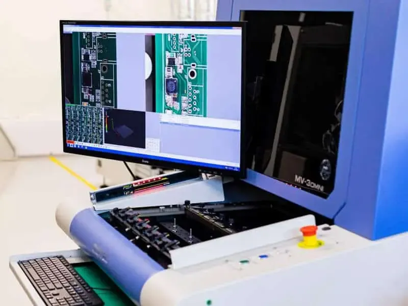
The core problem is visibility. Automated optical inspection (AOI) and manual visual inspection rely on optical access to solder fillets, component leads, and pad wetting. Once coating is applied, those features are partially or fully obscured. A marginal solder joint that would have been caught during pre-coat inspection now passes through the line and only fails later, either during electrical test or in the field.
Coating also changes the thermal and mechanical environment around components. The coating material has a different coefficient of thermal expansion (CTE) than the solder, the component lead frame, and the PCB laminate. During thermal cycling, this CTE mismatch applies mechanical stress to solder joints. If the joint already has poor wetting or voids, the coating can accelerate crack propagation rather than protect against it.
The second issue is chemical interaction. Solvent-based coatings can soften or swell certain component materials, particularly electrolytic capacitors, relays, and some connectors. Cure temperatures for urethane or silicone coatings can exceed the rated temperature of plastic packages or low-temperature solder alloys. You need to check every component's temperature rating against the coating cure profile before committing to a material.
The third issue is process sequencing. Coating before electrical test is a common mistake. If you coat first and then discover an open or short during test, you must strip the coating, repair the joint, re-clean the area, and re-apply coating. That process is slow, expensive, and prone to adhesion failure on the repaired area. For any board with moderate complexity, pre-coat electrical test is the safer sequence.
---
PCB Design Review Points That Determine Coating Risk
Component Clearance and Package Height
The first design review item is component clearance. Coating thickness typically ranges from 25 to 75 microns for acrylic or urethane, and from 10 to 25 microns for parylene. You need enough clearance around components for the coating to flow evenly without bridging adjacent leads.
Fine-pitch QFPs with 0.4 mm or 0.5 mm pitch are the highest risk. If the coating bridges two adjacent leads, you create a conductive path that can cause intermittent shorts, especially under humidity. The same applies to BGAs, though the risk is different: coating cannot flow under a BGA body, so the solder balls remain uncoated. That is acceptable for protection, but it means the coating does nothing for BGA joint reliability. You must rely entirely on the solder process quality for BGA joints.
For through-hole components, the lead protrusion height matters. If leads extend more than 1.5 mm above the board surface, spray coating may not cover the full lead height, leaving exposed metal that can corrode. Selective coating can address this, but it adds cost and requires a separate process step.
Review your component height data against the coating application method. Spray coating follows line-of-sight, so tall components create shadowing effects where the coating does not reach the board surface behind the component. Dip coating covers everything but requires masking of areas that must remain uncoated. Selective coating gives you the most control but requires a programming file that maps the exact coated and uncoated regions.
Pad Finish and Solderability
Pad finish directly affects whether the solder joint is sound before coating is applied. The common finishes are HASL, ENIG, ENEPIG, and OSP. Each has different wetting behavior and shelf life.
OSP is the most sensitive to storage and handling. If the board sits in inventory too long or goes through multiple reflow cycles, the OSP degrades and wetting suffers. Marginal wetting produces fillets that look acceptable under AOI but have poor intermetallic formation. Coating over those joints locks in the defect.
ENIG and ENEPIG are more forgiving because the nickel barrier layer provides consistent wetting. However, ENIG has a known risk of "black pad" — a brittle nickel-phosphorus layer that causes pad fracture. Black pad is not visible before soldering and can pass AOI after soldering. Coating over a black pad failure makes the problem worse because the crack is hidden and the coating may wick into the fracture.
Your design review should confirm that the pad finish matches the component finish and the soldering process. If you are using lead-free solder with OSP finish, verify the reflow profile is within the J-STD-020 moisture sensitivity level (MSL) requirements for all components. A board that has absorbed moisture before reflow can produce voids or popcorning in the package, and coating will not fix that.
Land Pattern Design and Solder Joint Geometry
IPC-7351 land patterns are the baseline for SMT footprint design. If your land patterns deviate from IPC-7351, you need to justify the deviation in the design review. The land pattern determines the solder joint geometry, which in turn determines whether the joint can tolerate the mechanical stress that coating introduces.
A common deviation is reducing the land pattern to save board space. This produces smaller fillets with less solder volume. The joint may pass electrical test but have reduced mechanical strength. When coating cures, it shrinks slightly and applies stress to the joint. A marginal joint can crack during cure or during the first thermal cycle.
Another issue is the solder paste aperture design. The stencil aperture should match the land pattern and the component lead geometry. If the aperture is too small, you get insufficient solder volume and poor fillet formation. If it is too large, you risk solder bridging, especially on fine-pitch components. Your EMS partner should review the stencil design against the land pattern and the coating thickness to ensure the final joint geometry has adequate solder volume.
---
Coating Material Selection and Its Impact on Assembly
Coating Types and Their Process Constraints
The four main coating types are acrylic, silicone, urethane, and parylene. Each has different properties that affect assembly risk.
| Coating Type | Typical Thickness | Cure Process | Key Assembly Risk |
|---|---|---|---|
| Acrylic | 25–75 microns | Solvent evaporation, room temperature or mild heat | Solvent can attack sensitive components; low abrasion resistance |
| Silicone | 50–200 microns | Heat cure or moisture cure | High CTE mismatch; can reflow during wave solder if applied before soldering |
| Urethane | 25–75 microns | Heat cure | High cure temperature may exceed component ratings; difficult to remove for rework |
| Parylene | 10–25 microns | Vacuum deposition | Requires masking of large areas; high equipment cost; excellent coverage but hard to inspect |
Acrylic is the most common because it is easy to apply, easy to rework, and has good dielectric properties. The risk is solvent attack on components. Check the material compatibility of electrolytic capacitors, plastic connectors, and any component with a non-hermetic package.
Silicone has the best high-temperature performance and good moisture resistance, but it has a high CTE. On a board with large BGAs or ceramic components, the CTE mismatch can cause solder joint stress during thermal cycling. Silicone is also soft, so it provides less mechanical protection against vibration.
Urethane has excellent abrasion and chemical resistance but requires a heat cure that can exceed 80°C. Check every component's maximum storage and operating temperature. Some plastic packages, especially those with low-cost molding compounds, can warp or delaminate at cure temperature.
Parylene is the premium option. It provides uniform coverage even under components, but it requires vacuum deposition and extensive masking. The masking process is a significant assembly risk because any mask misalignment leaves coating where it should not be, or leaves components uncoated where protection is required.
Specifying Coating in the RFQ
Your RFQ must include the coating specification so the assembler can plan the process. The minimum information is:
- Coating type (acrylic, silicone, urethane, parylene)
- Required thickness range
- Application method (spray, dip, selective, or vacuum deposition)
- Cure profile (temperature and time)
- Areas that must remain uncoated (test points, edge connectors, specific components)
- Whether coating is applied before or after electrical test
If you do not specify the coating type, the assembler will make a default choice that may not match your reliability requirements. If you do not specify the uncoated areas, the assembler will coat everything, which blocks test access and rework.
The cure profile is especially important. If you specify a urethane coating that requires an 80°C cure, the assembler must verify that all components on the board can tolerate that temperature. Some components, such as certain crystal oscillators or battery holders, have lower temperature ratings. The assembler may need to use a different coating or a selective application method to protect those components.
---
Inspection and Test Planning Around the Coating Step
Pre-Coating Inspection and Test
The pre-coating inspection is your last chance to catch solder defects while they are visible and reworkable. The sequence should be:
1. AOI after reflow to catch gross defects such as missing components, tombstoning, and solder bridges 2. X-ray inspection for BGAs, QFNs, and other components where solder joints are not visible 3. First-article inspection (FAI) to verify component placement, polarity, and solder joint quality against the BOM and assembly drawings 4. Electrical test (ICT or flying probe) to verify opens, shorts, and component values
This sequence follows the requirements of J-STD-001 for soldered electrical and electronic assemblies and IPC-A-610 for acceptability of electronic assemblies. The standards define the process requirements and acceptance criteria, but the practical point is that you must perform these steps before coating.
The FAI is critical for the first board from a new design. The inspector should verify that the component clearance matches the coating plan, that test points are accessible, and that no component is positioned where coating will interfere with its function. This is the time to catch design errors, not after coating is applied.
Post-Coating Inspection
After coating, you need a different inspection approach. AOI is less effective because the coating obscures solder joints. The post-coating inspection focuses on:
- Coating coverage: Are all required areas coated?
- Coating thickness: Is the thickness within specification?
- Coating defects: Are there bubbles, pinholes, or delamination?
- Uncoated areas: Are the masked areas clean and free of coating residue?
- Component damage: Did the coating process damage any components?
The post-coating inspection is typically a manual visual inspection with UV light if the coating contains a fluorescent tracer. Some coatings include a UV tracer specifically to make inspection easier. If your coating does not include a tracer, consider adding it to the specification.
Rework Considerations
Rework after coating is significantly more expensive and risky than rework before coating. The coating must be removed from the affected area, the solder joint repaired, the area cleaned, and the coating re-applied. Each step introduces risk of damage to adjacent components.
For this reason, the pre-coating electrical test is not optional for boards with moderate to high complexity. If you skip the pre-coating test to save cost, you accept the risk of discovering a defect after coating, which will cost more to repair than the test would have cost to perform.
---
Practical Example: Evaluating a Mixed-Technology Board
Consider a board with the following characteristics:
- 6-layer stackup, 1.6 mm total thickness, FR-4 laminate
- 1 oz copper on outer layers, 0.5 oz on inner layers
- Components: one 0.8 mm pitch BGA, two 0.5 mm pitch QFPs, several 0402 passives, and one through-hole connector
- ENIG pad finish
- Acrylic coating, 50 microns nominal thickness, spray application
- Coating applied after electrical test
The design review should check:
1. BGA clearance: The BGA has 0.8 mm pitch, which is coarse enough for reliable soldering. The coating will not flow under the BGA, so the solder balls remain uncoated. This is acceptable, but the BGA joint quality must be verified with X-ray before coating.
2. QFP clearance: The 0.5 mm pitch QFPs are the highest coating risk. The coating thickness of 50 microns is within the acceptable range, but the spray application must be controlled to avoid bridging between leads. The assembler should use selective spray or a mask over the QFP areas if bridging is a concern.
3. Test point access: The board has test points for ICT. These must be masked before coating. The RFQ should specify the exact test point locations and the masking method.
4. Connector protection: The through-hole connector must remain uncoated on the mating surface. The RFQ should specify that the connector is masked or that the coating is applied selectively to avoid the connector area.
5. Component temperature rating: The acrylic coating cures at room temperature, so there is no thermal risk to components. If the coating were urethane with a heat cure, the review would need to check every component's temperature rating.
The review should also verify that the stencil design provides adequate solder volume for the QFP and BGA joints. The stencil aperture ratio and aspect ratio should be checked against the land pattern and the component lead geometry.
---
Common Mistakes and When to Involve the Manufacturer
Mistake 1: Assuming Coating Fixes Solder Defects
Coating does not fix wetting problems, voids, insufficient fillets, or cold solder joints. It only hides them. If you have marginal solder joints, coating will make them harder to find and harder to repair. The solder process must be validated before coating is considered.
Mistake 2: Ignoring Component Height and Lead Pitch
Component height affects coating coverage in spray application. Tall components create shadowing. Fine-pitch leads are at risk of bridging. The design review must consider both factors together, not in isolation.
Mistake 3: Coating Before Electrical Test
Coating before test means you cannot access test points, and you cannot see the solder joints for rework. The test sequence should always be: solder, inspect, test, then coat.
Mistake 4: Not Specifying Coating in the RFQ
If the RFQ does not specify coating type, thickness, application method, cure profile, and uncoated areas, the assembler will make assumptions. Those assumptions may not match your reliability requirements. The RFQ must include the full coating specification.
When to Involve the Manufacturer
Involve your EMS partner early, ideally during the design review before the board is released to fabrication. The manufacturer can review the Gerber files, BOM, and coating specification for:
- Component clearance and coating compatibility
- Pad finish and solderability
- Stencil design and solder volume
- Test point access and masking requirements
- Cure temperature compatibility with component ratings
The manufacturer's DFM review is the last chance to catch coating-related risks before the board goes to production. After the board is fabricated and assembled, changes are expensive.
For related risk evaluation topics, see How to Evaluate SMT Assembly Risk from FOPLP and Thermal Processing Trends and How to Evaluate SMT Assembly Risk from PCB Design and Circuit Board Trends. For design entry considerations, review How to Evaluate SMT Assembly Risk from PCB Design and Circuit Symbols and How to Evaluate SMT Assembly Risk from PCB Design and KiCad Trends. Manufacturing-side factors are covered in How to Evaluate SMT Assembly Risk from PCB Design and PCB Manufacturing Trends.
---
FAQ
Why does conformal coating affect SMT assembly risk?
Conformal coating changes the thermal and mechanical environment around SMT components. If you apply it before validating the assembly process, you can trap flux residues, mask rework access, and hide defects that AOI would normally catch. Evaluate coating risk during PCB design by reviewing component clearance, pad finish, and whether the coating will be applied before or after test.
Where do engineers make mistakes when evaluating coating and SMT risk?
The most common mistake is assuming coating will protect a board that already has marginal solder joints. Coating does not fix wetting problems, voids, or insufficient fillets. Another mistake is ignoring component height and lead pitch when planning coating thickness, which can bridge fine-pitch QFPs or BGAs. Always review the coating type, application method, and cure profile against your component temperature ratings.
How can I verify coating and SMT risk before sending the PCBA to production?
Before the build, send your Gerber files, BOM, and a coating specification to your EMS partner. Ask them to run a DFM review that checks for component clearance, pad finish compatibility, and whether any components are sensitive to coating solvents or cure temperatures. Confirm that the coating will not interfere with test points, connectors, or mechanical features.
What coating information belongs in the RFQ for a turnkey PCBA assembly?
Your RFQ should include the coating type (acrylic, silicone, urethane, or parylene), required thickness, application method (spray, dip, or selective), and cure profile. Also list any areas that must remain uncoated, such as test points, edge connectors, or specific components. This information lets the assembler plan stencil design, reflow, and inspection around the coating step.
Does conformal coating affect inspection and testing during SMT assembly?
Yes, because coating can hide solder defects and make rework difficult. If you coat a board before full electrical test, you may not catch opens or shorts until after the coating is cured, which complicates repair. For high-reliability boards, perform first-article inspection and electrical test before coating, then do a final visual check after coating to verify coverage and adhesion.
How does the coating cure profile affect component selection?
The cure profile determines the maximum temperature and duration that components will experience after assembly. If the cure temperature exceeds a component's rated temperature, the component can be damaged. Check the datasheet for every component, especially plastic packages, electrolytic capacitors, and battery holders. If any component cannot tolerate the cure temperature, you must select a different coating or use a selective application method that avoids the sensitive component.
---
> Practical note: When you review a PCB design for coating compatibility, always check the component height data against the spray coating line-of-sight. A tall component can shadow the board surface behind it, leaving an uncoated area that corrodes over time. If you cannot avoid tall components, specify selective coating or a second pass with a different spray angle.
> Engineering handoff note: How to Evaluate SMT Assembly Risk from Solder Mask and Surface Finish Trends before the release package is frozen.
> Engineering handoff note: How to Evaluate SMT Assembly Risk from Acquisition and CEO Trends before the release package is frozen.
> Engineering handoff note: How to Evaluate SMT Assembly Risk from Automotive and ADAS Trends before the release package is frozen.