
Direkte Antwort
PCB Das Materialrisiko ist die Wahrscheinlichkeit, dass Ihre Laminatauswahl zu Herstellungsfehlern, Impedanzausfällen oder langfristigen Zuverlässigkeitsproblemen führt. Sie bewerten es, indem Sie Ihre Stapelanforderungen mit der Prozessfähigkeit, Materialverfügbarkeit und PTFE-spezifischen Handhabungskompetenz des Herstellers vergleichen, bevor Sie Gerbers freigeben. Eine strukturierte Überprüfung während RFQ, nicht nach der Erstmusterprüfung, ist die einzige Möglichkeit, diese Probleme zu erkennen, solange Änderungen noch kostengünstig sind.
Warum Materialrisiken ein Herstellungsproblem und nicht nur ein Designproblem sind
Ingenieure betrachten die Laminatbeschriftung in einer Zeichnung oft als feste Spezifikation. In Wirklichkeit bestimmt das von Ihnen ausgewählte Material, wie der Fab Shop Ihr Board verarbeiten kann. FR-4, Hochfrequenzlaminate und PTFE-basierte Materialien erfordern jeweils unterschiedliche Bohrparameter, Lochwandvorbereitung, Laminierungszyklen und Oberflächenbeschaffenheiten. Wenn Ihr Hersteller nicht über die richtige Ausrüstung oder Prozesserfahrung verfügt, kann es sein, dass die Platine die elektrischen Tests zwar besteht, aber bei thermischen Belastungen oder beim Zusammenbau versagt.
Das materielle Risiko zeigt sich auf verschiedene Weise:
- Impedanzschwankung aufgrund von Harzgehaltsänderungen im gesamten Panel
- Bohrfehler wie Schlieren oder raue Lochwände in PTFE-Materialien
- Delamination beim Reflow- oder thermischen Belastungstest
- Feuchtigkeitsaufnahme führt zu einer Abweichung der elektrischen Leistung
- Verzögerungen bei der Beschaffung, wenn eine bestimmte Laminat-Teilenummer nicht verfügbar ist
Der häufigste Fehler besteht darin, die Materialauswahl als eine rein elektrische Entscheidung zu betrachten. Ein Laminat, das Ihnen die richtige Dielektrizitätskonstante und den richtigen Verlustfaktor bietet, lässt sich möglicherweise nicht mit dem Standardfluss Ihres Herstellers verarbeiten. Die Bewertung muss eine gemeinsame Übung zwischen Ihrer Entwurfsabsicht und den tatsächlichen Fähigkeiten des Herstellers sein.
Beim Stackup beginnt das Risiko
Jede Materialrisikobewertung sollte mit der Stapelung beginnen. Das Harzsystem, der Glasstil und das Kupfergewicht sind keine unabhängigen Entscheidungen. Sie interagieren miteinander und mit dem Herstellungsprozess.
Beispielsweise reicht ein Kupfergewicht von 0,5 Unzen auf einer Außenschicht möglicherweise für das Routing mit feinem Rastermaß aus, es besteht jedoch ein höheres Risiko für Faltenbildung in der Kupferfolie beim Laminieren. Ein dünnes Prepreg mit einem Glasstil mit hohem Harzgehalt bietet möglicherweise die erforderliche Impedanz, kann jedoch anfällig für Harzmangel an den Kanten der Platine sein. Das DFM-Team des Herstellers wird sich diese Interaktionen ansehen, aber nur, wenn Sie ihnen während des RFQ den vollständigen Stackup geben.
Der Glasstil ist wichtiger, als den meisten Ingenieuren bewusst ist. E-Glas, S-Glas und L-Glas haben unterschiedliche Dielektrizitätskonstanten und Verlustfaktor. Der Webstil beeinflusst das Glas-Harz-Verhältnis, was wiederum Auswirkungen auf die effektive Dielektrizitätskonstante und die Impedanzkonsistenz über das gesamte Panel hat. Wenn Sie ein Material angeben, das der Hersteller nicht auf Lager hat, kann der Ersatz durch eine andere Glasart Ihre Impedanz um 3–5 Ohm ändern.
Wie PTFE-Laminate das Risikoprofil verändern
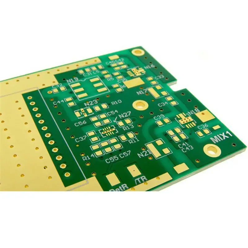
PTFE und andere Hochfrequenzlaminate lösen echte elektrische Probleme. Bei Frequenzen über 5 GHz weist der Standard FR-4 einen Verlustfaktor auf, der für viele Anwendungen einfach zu hoch ist. Aber PTFE birgt völlig andere Herstellungsrisiken.
PTFE ist weich und kratzt leicht. Es nimmt Feuchtigkeit mit einer Geschwindigkeit auf, die deutlich höher ist als FR-4. Es erfordert spezielle Bohrparameter, da es im Gegensatz zu glasfaserverstärktem Epoxidharz nicht absplittert. Die Lochwände müssen mit Plasma behandelt oder mit Natrium geätzt werden, bevor die Kupferbeschichtung haftet. Wenn einer dieser Schritte übersprungen oder falsch ausgeführt wird, werden Sie eine schlechte Lochwandqualität, Hohlräume in der Beschichtung oder Delaminierung bei thermischer Belastung feststellen.
Das Risiko liegt nicht nur im Material selbst. Es liegt in der Erfahrung des Herstellers damit. In einem Betrieb, der hauptsächlich FR-4-Boards verwendet, sind möglicherweise nicht die Prozessparameter für PTFE eingestellt. Möglicherweise verfügen sie nicht über die richtigen Bohrer, die richtigen Spindelgeschwindigkeiten oder die richtige Plasmaätzausrüstung. Sie sollten den Hersteller direkt nach seinen Erfahrungen mit PTFE-Prozessen fragen und Referenzen oder Testdaten anfordern.
Feuchtigkeits- und Handhabungsrisiken
PTFE-Laminate absorbieren Feuchtigkeit aus der Luft. Wenn die Platinen vor dem Laminieren oder vor dem Auftragen der Lötmaske nicht gebrannt werden, kann sich die eingeschlossene Feuchtigkeit beim Reflow ausdehnen und Blasenbildung verursachen. Die Handhabungsanforderungen unterscheiden sich von FR-4:
- Platten müssen vor der Verarbeitung trocken gelagert oder gebrannt werden
- Bohren erfordert niedrigere Vorschübe und höhere Spindelgeschwindigkeiten
- Die Vorbereitung der Lochwand erfordert Plasmaätzen oder eine chemische Behandlung auf Natriumbasis
- Die Auswahl der Oberflächenbeschaffenheit ist wichtig, da die Haftung auf PTFE schwächer ist
Eine praktische Faustregel besagt, dass PTFE-Platten länger als FR-4 bei niedriger Temperatur gebacken werden sollten. Das genaue Profil hängt vom Material und der Ausstattung des Herstellers ab und muss daher bei der DFM-Überprüfung bestätigt werden.
> Practical note: If your design requires PTFE, ask the manufacturer for a cross-section of a test coupon from a recent PTFE build. This will show you the hole wall quality and plating adhesion before you commit to a full production run.
Der RFQ als Materialrisiko-Tool
Der RFQ ist die erste und beste Gelegenheit, wesentliche Risiken zu bewerten. Die meisten Ingenieure schicken einen Aufbau und eine Reihe elektrischer Anforderungen und erwarten ein Angebot. Ein effektiverer Ansatz besteht darin, die spezifischen Materialangaben aufzunehmen und den Hersteller zu bitten, die Prozessfähigkeit zu bestätigen.
Zu den Informationen, die in den RFQ für die Bewertung wesentlicher Risiken gehören, gehören:
- Genaue Laminat-Teilenummer und Hersteller
- Glasstil und Harzsystem
- Kupfergewicht für jede Schicht
- Zielimpedanz und Toleranz
- Betriebsfrequenz und thermische Umgebung
- Anforderungen an Zuverlässigkeitstests
- Panelgröße und -menge
Wenn Sie diese Informationen bereitstellen, kann der Hersteller das Risiko des Materials anhand seines Prozesses bewerten. Sie können Ihnen sagen, ob das Material vorrätig ist, ob sie Erfahrung damit haben und ob Ihre Anforderungen angepasst werden müssen.
Was Sie dem Hersteller fragen sollten
Während der RFQ-Phase sollten Sie spezifische Fragen zum materiellen Risiko stellen:
1. Is the laminate part number in stock or does it require a special order? 2. What is the lead time for the material and the build? 3. Do you have process experience with this resin system? 4. What is your capability for PTFE drilling and plating? 5. Can you confirm the impedance tolerance you can hold with this material? 6. What surface finish is compatible with this laminate?
Die Antworten auf diese Fragen verraten Ihnen mehr über das tatsächliche Risiko als jedes Datenblatt. Ein Hersteller, der zögert oder vage Antworten zu PTFE-Erfahrungen gibt, ist ein Warnsignal.
Materialsubstitutionen und ihre versteckten Risiken
Materialsubstitutionen sind eine häufige Risikoquelle. Wenn ein bestimmtes Laminat nicht verfügbar ist, kann der Hersteller einen Ersatz vorschlagen. Der Ersatz kann eine ähnliche Dielektrizitätskonstante haben, aber möglicherweise einen anderen Verlustfaktor, eine andere Feuchtigkeitsabsorptionsrate oder einen anderen Wärmeausdehnungskoeffizienten.
Eine Substitution, die die Dielektrizitätskonstante nur um 0,2 ändert, kann die Impedanz einer Leiterbahn mit kontrollierter Impedanz um 2–3 Ohm verschieben. Bei manchen Designs kann das innerhalb der Toleranz liegen, bei anderen jedoch nicht. Ein Austausch, der den CTE verändert, kann dazu führen, dass sich die Platine während der Montage verbiegt oder verdreht, insbesondere wenn die Platine groß ist oder eine dicke Kupferverteilung aufweist.
Sie sollten jede vorgeschlagene Substitution als neues Ereignis mit wesentlichem Risiko behandeln. Der Hersteller sollte das Datenblatt des Ersatzes bereitstellen und Sie sollten bestätigen, dass die elektrischen und thermischen Anforderungen weiterhin erfüllt sind. Wenn die Ersetzung nach dem RFQ vorgeschlagen wird, sollten Sie eine neue Impedanzberechnung und einen thermischen Belastungstest anfordern.
Ein praktischer Rahmen für die Prüfung materieller Risiken
Eine strukturierte Materialrisikoprüfung sollte vor der Veröffentlichung von Gerber erfolgen. Die folgenden Schritte helfen Ihnen, das Risiko systematisch einzuschätzen.
Schritt 1: Definieren Sie die elektrischen und thermischen Anforderungen
Beginnen Sie mit der Betriebsfrequenz, der Zielimpedanz, der thermischen Umgebung und den erwarteten Zuverlässigkeitstests. Diese Anforderungen bestimmen, welche Materialfamilien überhaupt realisierbar sind.
Schritt 2: Wählen Sie die Materialfamilie aus
Wählen Sie basierend auf den Anforderungen eine Materialfamilie: FR-4, Hoch-Tg FR-4, Rogers, PTFE oder einen Hybrid. Springen Sie nicht zu einer bestimmten Teilenummer, ohne die Auswirkungen auf den Prozess zu berücksichtigen.
Schritt 3: Bestätigen Sie das Material beim Hersteller
Senden Sie die Materialaufforderung während des RFQ an den Hersteller. Fordern Sie eine Bestätigung der Verfügbarkeit, Durchlaufzeit und Prozessfähigkeit an. Wenn es sich bei dem Material nicht um Standardmaterial handelt, fragen Sie nach der Lieferzeit und einer etwaigen Mindestbestellmenge.
Schritt 4: Überprüfen Sie das DFM-Feedback
Wenn der Hersteller den DFM zurückgibt, achten Sie auf materialspezifische Kommentare. Dazu können Warnungen zum Lochseitenverhältnis, Kompatibilitätsprobleme mit der Oberflächenbeschaffenheit oder Empfehlungen für ein anderes Laminat gehören. Ignorieren Sie diese Kommentare nicht.
Schritt 5: Fordern Sie einen Testcoupon an
Für Materialien mit hohem Risiko wie PTFE fordern Sie auf dem Panel einen Testcoupon an. Dies ermöglicht es dem Hersteller, die Impedanz zu messen, die Lochqualität zu prüfen und einen thermischen Belastungstest durchzuführen, bevor die gesamte Platine zusammengebaut wird.
Schritt 6: Dokumentieren Sie die Risikoentscheidung
Notieren Sie die Materialauswahl, die Bestätigung des Herstellers und etwaige Annahmen. Diese Dokumentation ist hilfreich, wenn das Material später ersetzt wird oder ein Zuverlässigkeitsproblem auftritt.
Häufige Fehler bei der Materialrisikobewertung
Ingenieure machen bei der Bewertung materieller Risiken immer wieder dieselben Fehler. Die häufigsten sind:
- PTFE wie FR-4 behandeln: PTFE erfordert unterschiedliche Bohrungen, Beschichtungen und Handhabung. Wenn Sie dies nicht berücksichtigen, kommt es zu schlechter Lochqualität und Delaminierung.
- Verfügbarkeit ignorieren: Ein Material, das nicht auf Lager ist, kann die Lieferzeit um Wochen verlängern. Überprüfen Sie die Verfügbarkeit, bevor Sie sich auf das Design festlegen.
- Angenommen, das Datenblatt ist die ganze Geschichte: Das Datenblatt gibt Ihnen die Eigenschaften des Materials, aber nicht die Fähigkeit des Herstellers, es zu verarbeiten.
- Keine Testcoupons anfordern: Ein Testcoupon ist eine kostengünstige Möglichkeit, das Material und den Prozess vor dem vollständigen Bau zu überprüfen.
- Akzeptieren eines Ersatzes ohne Neubewertung: Ein Ersatzmaterial kann ähnliche elektrische Eigenschaften, aber ein unterschiedliches thermisches oder mechanisches Verhalten haben.
Standards und Referenzrahmen
IPC-4101 ist die Spezifikation für Laminatmaterialien. Es definiert die Anforderungen an Grundmaterialien, einschließlich der Glasübergangstemperatur, der Dielektrizitätskonstante und des Verlustfaktors. Wenn Sie ein Laminat angeben, sollten Sie auf das Schrägstrichblatt IPC-4101 verweisen, das für das Material gilt.
IPC-6012 deckt die Qualifikation und Leistung starrer PCBs ab. Es definiert die Anforderungen an die fertige Platine, einschließlich der Beschichtung, des Leiterabstands und der thermischen Belastungsleistung. Wenn Sie Bedenken hinsichtlich eines wesentlichen Risikos haben, sind die Anforderungen von IPC-6012 die Akzeptanzkriterien.
IPC-TM-650 ist die Testmethodenfamilie. Es umfasst Methoden zur Messung der Dielektrizitätskonstante, des Verlustfaktors, der Schälfestigkeit und der thermischen Spannung. Wenn Sie den Hersteller nach Testdaten fragen, verweisen Sie auf die entsprechende Methode IPC-TM-650.
Diese Standards stellen eine gemeinsame Sprache zwischen Ihnen und dem Hersteller dar. Sie ersetzen nicht die Notwendigkeit eines direkten Gesprächs über die Prozessfähigkeit, geben Ihnen aber eine Grundlage dafür, was akzeptabel ist.
Wesentliches Risiko im Kontext anderer Herstellungsrisiken
Materielles Risiko existiert nicht isoliert. Es interagiert mit anderen Fertigungsrisiken, wie Laminierungs- und Prepreg-Trends, SMT-Montage und fortschrittlichen Technologien wie HDI und Starrflex. Beispielsweise kann ein Material, das schwer zu verarbeiten ist, auch schwierig zu montieren sein. Das Reflow-Profil SMT ist möglicherweise nicht mit der Feuchtigkeitsempfindlichkeit des Materials kompatibel.
Wenn Sie an einem Hochfrequenzdesign arbeiten, sollten Sie auch prüfen, wie sich die Materialauswahl auf den SMT Montageprozess auswirkt. Das gleiche Materialrisiko, das sich auf die PCB-Fertigung auswirkt, wirkt sich auch auf die Baugruppenausbeute aus. Das Reflow-Profil, die Oberflächenbeschaffenheit und das Komponentenpaket interagieren alle mit dem Material.
Einen umfassenderen Überblick darüber, wie sich die Auswahl von Laminierungen und Prepregs auf das Risiko auswirkt, finden Sie in unserem Leitfaden zum Thema „So bewerten Sie PCB Materialrisiken durch Laminierungs- und Prepreg-Trends“ (/pcb-manufacturing/how-to-evaluate-pcb-materials-risk-from-lamination-and-prepreg-trends). Hier wird die Wechselwirkung zwischen Harz und Glas ausführlicher behandelt.
Wenn Sie ein Design bewerten, das den SMT Zusammenbau durchläuft, ist das Materialrisiko nur ein Teil der Gleichung. Auch die Bauteilplatzierung, die Lotpaste und das Reflow-Profil bergen Risiken. Unter How to Evaluate SMT Assembly Risk from PCB Manufacturing and Sourcing Trends finden Sie ein Framework, das die Montageseite abdeckt.
Bei HDI- und Starrflex-Projekten erhöht sich das Materialrisiko durch die Komplexität des Baus. Die Laminierungszyklen, das Laserbohren und der sequentielle Aufbau erhöhen das Risiko. Unter So bewerten Sie das Risiko fortgeschrittener PCB-Technologie für HDI- und starr-flexible Projekte finden Sie einen Überprüfungsprozess, der diese fortschrittlichen Technologien behandelt.
Wenn Ihr Design Flex oder Starrflex beinhaltet, ist die Materialauswahl noch wichtiger. Das flexible Material muss sich biegen, ohne zu reißen, und das Klebesystem muss die Laminierung überstehen. Sehen Sie sich den Flex PCB Herstellungsprozess: Materialauswahl, Ätzen und Laminieren an, um einen detaillierten Einblick in die Verarbeitung flexibler Materialien zu erhalten.
Einen anderen Blickwinkel auf das Montagerisiko finden Sie unter How to Evaluate SMT Assembly Risk from PCB Assembly and COB Trends, wo die Chip-on-Board- und Assembly-Trends behandelt werden, die mit der Materialauswahl interagieren.
Ein konkretes Beispiel für eine Materialrisikobewertung
Stellen Sie sich ein Design vor, das eine kontrollierte Impedanz von 50 Ohm auf einer 1,6-mm-Platine mit einer Zielfrequenz von 10 GHz erfordert. Der Ingenieur wählt ein PTFE-Laminat mit einer Dielektrizitätskonstante von 3,0 und einem Verlustfaktor von 0,001.
Der Aufbau besteht aus einer 4-Lagen-Platine mit 0,5 Unzen Kupfer auf den Außenschichten und 1 Unzen Kupfer auf den Innenschichten. Die Dicke des Dielektrikums beträgt 0,4 mm zwischen der Signal- und der Referenzebene.
Die Bewertung des materiellen Risikos würde wie folgt ablaufen:
1. Electrical check: The dielectric constant of 3.0 and the thickness of 0.4 mm give a trace width of approximately 0.3 mm for a 50-ohm impedance. This is a reasonable trace width for the design.
2. Process check: The manufacturer confirms that they have PTFE experience and that the material is in stock. They note that the hole aspect ratio for the board is 8:1, which is within their capability.
3. Reliability check: The manufacturer recommends a test coupon for thermal stress. The board will be subjected to a 288°C solder float test per IPC-TM-650.
4. Sourcing check: The material is available with a lead time of 2 weeks. The manufacturer confirms that no substitution is required.
Das Risiko wird als gering eingeschätzt. Der Entwurf wird mit der Version Gerber fortgesetzt.
Wenn der Hersteller gesagt hätte, dass das Material nicht auf Lager sei und eine Vorlaufzeit von 6 Wochen benötige, wäre das Risiko hoch. Der Ingenieur müsste ein Ersatzmaterial oder einen anderen Designansatz in Betracht ziehen.
FAQ
Warum ist das Materialrisiko PCB in der Fertigung wichtig?
Die Materialauswahl beeinflusst die Impedanzkontrolle, die thermische Zuverlässigkeit und die Fertigungsausbeute. Ein Laminat, das schwer zu beschaffen oder zu verarbeiten ist, kann die Produktion verzögern und die Kosten erhöhen. Eine frühzeitige Risikobewertung verhindert Überraschungen bei der Fertigung und Montage.
Welche häufigen Fehler machen Ingenieure bei PTFE-Laminaten?
Ingenieure behandeln PTFE oft wie Standard FR-4. PTFE ist weich, nimmt Feuchtigkeit auf und erfordert vor dem Plattieren eine spezielle Bohr- und Plasmabehandlung. Das Überspringen dieser Schritte führt zu schlechter Lochwandqualität und Delaminierung. Stellen Sie immer sicher, dass der Hersteller Erfahrung mit PTFE-Prozessen hat.
Wie kann ich das materielle Risiko überprüfen, bevor ich einen PCB erstelle?
Senden Sie Ihre Stapel- und Materialinformationen während RFQ an den Hersteller. Fordern Sie eine Bestätigung der Verfügbarkeit, Durchlaufzeit und Prozessfähigkeit an. Überprüfen Sie das DFM-Feedback des Herstellers auf materialspezifische Bedenken wie Lochseitenverhältnis oder Oberflächenkompatibilität.
Welche Informationen gehören in den RFQ für die Materialrisikobewertung?
Geben Sie die genaue Teilenummer des Laminats, den Glasstil, das Harzsystem, das Kupfergewicht und die Zielimpedanz an. Geben Sie außerdem die Betriebsfrequenz, die thermische Umgebung und etwaige Zuverlässigkeitstestanforderungen an. Dadurch kann der Hersteller die Materialeignung und das Prozessrisiko beurteilen.
Wie wirken sich PTFE-Trends auf das PCB Materialrisiko aus?
Mit steigenden Datenraten und HF-Frequenzen werden immer häufiger PTFE und andere Hochfrequenzlaminate verwendet. Dies erhöht die Nachfrage nach spezialisierten Fertigungsverfahren. Im Vergleich zu FR-4 müssen Ingenieure mit längeren Vorlaufzeiten, höheren Kosten und strengeren Prozesskontrollen rechnen.
Wann sollte ich den Hersteller in die Materialprüfung einbeziehen?
Beziehen Sie den Hersteller ein, sobald Sie einen vorläufigen Überblick haben, idealerweise vor der Veröffentlichung von Gerber. Je früher Sie den Materialhinweis weitergeben, desto mehr Zeit hat der Hersteller, auf Probleme hinzuweisen und Alternativen vorzuschlagen. Ein Hersteller wie Omini kann DFM Feedback geben, das wesentliche Risiken erkennt, bevor sie zu einem Ertragsproblem werden.
> Engineering handoff note: How to Evaluate SMT Assembly Risk from PCB Fabrication and Sourcing Trends before the release package is frozen.
> Engineering handoff note: How to Evaluate Advanced PCB Technology Risk from High-Speed PCB and Integrity Trends before the release package is frozen.
> Engineering handoff note: How to Evaluate SMT Assembly Risk from PCB Manufacturing and Renewable Energy Trends before the release package is frozen.