
Direct Answer
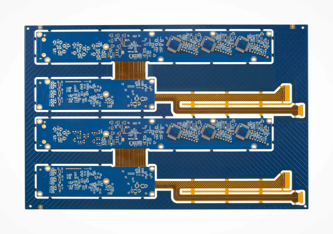
For most flexible LED PCB designs, start with a polyimide (PI) substrate, 1 oz (35 µm) electro-deposited (ED) copper, and a PI coverlay. This combination provides the best balance of solderability, bend life, and cost for typical LED strip applications. Switch to rolled-annealed (RA) copper when the board undergoes repeated dynamic flexing, and consider PET only for static, low-temperature assemblies where cost reduction outweighs thermal risk.
---
The Material Selection Framework: Start with the Bend Requirement
The first decision in flexible LED PCB material selection is not about the substrate—it is about the mechanical environment. Define whether the board will experience dynamic flexing (bending during operation, repeated cycles) or static flexing (bent once during installation and then held in place). This single distinction drives nearly every subsequent material choice.
Dynamic flex applications, such as wearable LED arrays, moving cable assemblies, or foldable displays, require materials that can withstand repeated strain without fatigue failure. Static applications, such as edge-lit signage, architectural lighting profiles, or fixed backlight modules, allow more cost-optimized material choices because the copper and adhesive systems face only one-time deformation.
A practical rule: if the bend radius is smaller than 10 times the total board thickness, or if the board will flex more than 1,000 cycles in its lifetime, treat it as a dynamic flex design. This classification determines whether you can use standard ED copper or must pay the premium for RA copper.
Polyimide vs. PET: The Cost-Performance Tradeoff
Polyimide (PI) remains the default substrate for flexible LED PCBs because of its thermal stability (continuous operating range typically from −40°C to 150°C or higher, depending on grade), dimensional stability during soldering, and resistance to flex fatigue. PI withstands lead-free reflow profiles without significant shrinkage or warpage, which is critical when the PCB carries surface-mount LEDs.
Polyethylene terephthalate (PET) offers a lower material cost, but it introduces three practical problems. First, PET cannot survive standard lead-free reflow temperatures (peak 245–260°C) without deformation. Second, PET has higher moisture absorption, which can cause delamination in humid environments. Third, PET's lower glass transition temperature limits the LED power density you can dissipate through the substrate.
Use PET only when the LED strip is assembled with conductive adhesive or low-temperature solder (below 180°C), the operating environment stays below 85°C, and the product has no dynamic flex requirement. If you are uncertain about the assembly profile, ask your EMS partner to confirm the soldering method before committing to PET. For a broader comparison of substrate options, see our guide on Comparing Different Types of Printed Circuit Board Materials.
PI-PI vs. PI on Polyglass: When to Upgrade the Laminate
Standard flexible PCB laminates use a PI film bonded to a glass-reinforced epoxy or a polyglass carrier. For most LED strips, this construction is sufficient. However, when the LED power exceeds approximately 0.5 W per LED, or when the assembly will pass through multiple high-temperature reflow cycles, consider a PI-PI laminate where both the dielectric and the carrier are polyimide.
PI-PI laminates offer better dimensional stability, lower Z-axis expansion, and improved resistance to CAF (conductive anodic filament) growth in high-humidity environments. The tradeoff is cost—PI-PI typically costs 20–40% more than PI-on-polyglass. For high-brightness LED applications, also evaluate whether a metal-core flex base or an insulated metal substrate (IMS) provides better thermal management. These hybrid constructions combine a thin copper or aluminum base with a flex circuit layer, offering both flexibility in specific regions and heat spreading where the LEDs are densely packed. Copper Core PCBs: Revolutionizing the Electronics Industry explains how metal-core constructions handle thermal dissipation in LED applications.
---
Copper Weight and Foil Type: Controlling Resistance and Bend Fatigue
Copper selection involves two independent variables: weight (thickness) and foil type (ED vs. RA). Both affect electrical performance, mechanical reliability, and manufacturing yield.
Copper Weight: 1 oz Is the Default, But Calculate the Drop
Standard 1 oz (35 µm) copper is the right starting point for most flexible LED PCBs. It carries typical LED strip currents (0.3–1.5 A per meter for common 5050 or 2835 LED densities) with acceptable voltage drop over short runs. However, for long strips (above 2 meters) or high-current applications, the voltage drop in the return trace becomes significant.
A practical calculation: a 1 oz copper trace that is 1 mm wide has a resistance of approximately 0.5 Ω per meter. At 1 A, this creates a 0.5 V drop per meter—enough to cause visible brightness variation between the beginning and end of a long strip. Instead of widening the trace (which increases capacitance and consumes flex area), consider increasing copper weight to 2 oz (70 µm) in the return leg only. This hybrid copper weight approach reduces resistance without sacrificing flexibility in the signal traces.
Thin copper (0.5 oz or 18 µm) reduces the minimum via aperture and improves fine-pitch routing, but it becomes fragile under repeated bending. If your design requires 0.5 oz copper for routing density, verify that the dynamic flex regions do not contain vias or abrupt width transitions.
ED vs. RA Copper: The Bend Life Decision
Electro-deposited (ED) copper has a columnar grain structure that makes it stiffer and more prone to crack initiation under repeated bending. Rolled-annealed (RA) copper has a wrought, elongated grain structure that withstands flex fatigue significantly better—typically 10 to 100 times more bend cycles depending on the bend radius and stackup.
For static LED strips that bend once during installation, ED copper is acceptable and costs less. For dynamic applications, RA copper is mandatory. The cost premium for RA copper is typically 15–30% over ED, which is justified when the product must survive thousands of flex cycles.
A common mistake is using RA copper only in the dynamic flex region but keeping ED copper in the rigid sections. While this hybrid approach is possible, it requires a bonded or laminated transition that adds manufacturing complexity. Most EMS providers prefer a uniform copper type across the entire flex circuit to avoid registration issues during lamination.
---
Coverlay and Adhesive: Protecting Traces Without Blocking Light
The coverlay (also called coverfilm) is the insulating layer that protects the copper traces on a flexible PCB. Unlike a rigid PCB solder mask, the coverlay is a laminated film that requires an adhesive layer. Both the coverlay thickness and the adhesive system affect LED performance and assembly reliability.
Coverlay Thickness and LED Cavity Design
For LED applications, the coverlay must be opened (laser-cut or punched) to expose the LED pads and create a cavity for the LED package. The coverlay thickness directly affects the cavity depth, which in turn influences the light emission angle and brightness.
A standard coverlay is 1 mil (25 µm) PI with 1 mil (25 µm) adhesive, giving a total of 2 mil (50 µm). For shallow cavities where the LED lens should sit close to the surface, use a thinner coverlay—0.5 mil PI with 0.5 mil adhesive. The tradeoff is reduced mechanical protection for the traces and a more challenging laser-cutting process with tighter tolerance control.
Over-thick coverlay (2 mil PI plus 2 mil adhesive, totaling 4 mil or 100 µm) creates a deep cavity that can shadow the LED emission, reducing brightness by 10–20% depending on the LED viewing angle. If the LED has a wide viewing angle (120° or more), the cavity walls will block a portion of the emitted light. For side-emitting LEDs, the cavity design is even more critical—the coverlay opening must align precisely with the emission window.
Adhesive Systems: Acrylic vs. Epoxy
Two adhesive systems dominate flexible PCB coverlay lamination: acrylic and epoxy. Acrylic adhesives offer good flexibility and peel strength but have higher moisture absorption and lower thermal stability. Epoxy adhesives provide better thermal performance and lower outgassing but are stiffer and more prone to cracking under repeated flex.
For LED applications with operating temperatures above 100°C, specify an epoxy adhesive system. For dynamic flex applications, acrylic adhesives are often preferred because of their flexibility, but verify that the operating temperature stays below the adhesive's continuous rating. The adhesive also affects the minimum bend radius—a thicker adhesive layer increases the neutral axis offset and reduces the achievable bend radius before copper cracking occurs.
A practical note on coverlay alignment: the coverlay opening tolerance is typically ±0.1 mm for laser-cut openings. If the LED cavity must be tight (for example, a 0.2 mm clearance around a 3.5 mm × 3.5 mm LED package), this tolerance consumes a significant portion of the available margin. Discuss the alignment tolerance with your fabricator during DFM review, and consider increasing the cavity size by 0.1 mm per side to accommodate registration variation.
---
Thermal Management: When Standard Flex Materials Are Not Enough
Flexible LED PCBs face a fundamental thermal challenge: polyimide has a thermal conductivity of approximately 0.12–0.2 W/m·K, which is far lower than the 1–3 W/m·K of FR-4 and orders of magnitude below aluminum (200+ W/m·K). For low-power LEDs (below 0.1 W per LED), this is acceptable because the heat dissipates through the LED pads and into the surrounding air. For higher-power LEDs, the flex substrate becomes a thermal bottleneck.
Thermal Vias and Copper Spreading
The first thermal improvement is to maximize copper coverage under the LED. Use a thermal pad connected to a large copper pour on the backside of the flex circuit. Thermal vias (microvias or laser-drilled vias) can transfer heat from the LED pad to the backside copper, but they add manufacturing cost and reduce flex life. For dynamic flex regions, avoid thermal vias entirely—they create stress concentration points that initiate cracks.
Metal-Core Flex Hybrids
For LED modules with power above 0.5 W per LED, consider a hybrid construction: a thin copper or aluminum core bonded to a flex circuit. This provides the thermal spreading of a metal-core PCB with the flexibility of a polyimide circuit in designated bend regions. The metal core is typically 0.3–0.8 mm thick, and the flex circuit is laminated to it with a thermally conductive adhesive (1–3 W/m·K).
This hybrid approach is common in automotive interior lighting, where LEDs operate at moderate power and the assembly must fit into curved surfaces. The tradeoff is increased thickness and reduced overall flexibility—the metal core limits the minimum bend radius of the entire assembly. If the product requires both high LED power and tight bend radii, evaluate whether a rigid-flex construction with a metal-core rigid section is more appropriate.
Thermal Interface Materials and Heat Sinking
For LED strips mounted on aluminum extrusion profiles (common in architectural lighting), the flex PCB's thermal path includes the adhesive between the PCB and the extrusion. Standard acrylic PSA (pressure-sensitive adhesive) has low thermal conductivity (0.1–0.2 W/m·K) and creates a significant thermal barrier. Specify a thermally conductive PSA (0.5–1.5 W/m·K) or a mechanical clamping system with a thermal pad for higher-power applications.
The operating temperature range of the entire stackup—LED junction, solder joint, copper trace, substrate, adhesive, and heat sink—must be reviewed during design. Provide the recommended operating temperature range and minimum bend radius in the stackup drawing so the manufacturer can verify that the selected materials meet the requirements.
---
Manufacturing and DFM Considerations for Flexible LED PCBs
Material selection directly affects manufacturing yield and assembly reliability. Several DFM (Design for Manufacturing) issues commonly cause rework when the material choice is not aligned with the fabrication process.
Solder Stencil and Step Soldering
Flexible PCBs require a different solder stencil approach than rigid boards. The stencil must accommodate the flex material's thickness variation and the potential for warpage during reflow. For LED strips with mixed component sizes (small 0402 resistors alongside large 5050 LEDs), consider a step stencil with different solder paste thicknesses. This requires the EMS provider to have step-stencil capability and to verify that the flex material can withstand the additional pressure during printing.
Component Placement and Dynamic Flex Regions
SMT components should not be placed in dynamic flex regions. The solder joints create stress concentration points that fail under repeated bending. A common rule is to keep a 2–3 mm clearance between the edge of any component and the beginning of the dynamic bend region. If components must be placed near a bend line, use a strain-relief design with a gradual transition rather than an abrupt bend.
Coverlay Registration and LED Cavity Inspection
The coverlay opening alignment is critical for LED pads. Misregistration of the coverlay can cause solder to wick under the coverlay, creating shorts or reducing the effective pad area. During incoming inspection, the EMS provider should verify coverlay alignment using optical inspection. For LED cavities, the inspection must confirm that the opening is fully clear and that no adhesive residue remains on the copper pads—adhesive contamination causes poor wetting and solder joint voids.
Common DFM Mistakes That Create Rework
- Specifying a bend radius smaller than the material's minimum without verifying the stackup thickness
- Using ED copper in a dynamic flex region because the cost was not reviewed against the reliability requirement
- Selecting PET for a design that requires lead-free reflow soldering
- Over-thick coverlay that blocks LED emission, discovered only during photometric testing
- Missing thermal relief on large copper pours, causing tombstoning of small components during reflow
- No bend radius or flex cycle specification in the fabrication drawing, leaving the manufacturer to optimize for static life
For a complete overview of how flexible PCBs fit into the broader manufacturing flow, review the Circuit Board Manufacturing Process: A practical reference for Beginners. Understanding the lamination, drilling, and surface finish steps helps you specify materials that are compatible with the fabrication line.
---
Decision Table: Material Selection by Application
| Application Type | Substrate | Copper Type | Copper Weight | Coverlay | Adhesive | Notes |
|---|---|---|---|---|---|---|
| Static LED strip, decorative, low power (<0.1 W/LED) | PI or PET (if low-temp assembly) | ED | 1 oz | 1 mil PI + 1 mil adhesive | Acrylic | PET only if reflow <180°C |
| Static LED strip, standard power (0.1–0.5 W/LED) | PI | ED | 1 oz | 1 mil PI + 1 mil adhesive | Acrylic or epoxy | Verify thermal path to heat sink |
| Dynamic flex, wearable or moving cable | PI | RA | 1 oz | 0.5–1 mil PI + 0.5–1 mil adhesive | Acrylic | No vias in bend region |
| High brightness (>0.5 W/LED) | PI-PI or metal-core hybrid | RA (for flex sections) | 1–2 oz | 1 mil PI + 1 mil adhesive | Epoxy | Consider IMS for rigid sections |
| Long strip (>2 m), high current | PI | ED or RA | 2 oz in return leg | 1 mil PI + 1 mil adhesive | Epoxy | Calculate voltage drop first |
| Automotive interior, curved mounting | PI-PI with metal-core rigid section | RA | 1 oz | 1 mil PI + 1 mil adhesive | Epoxy | Verify thermal cycling range |
---
What to Verify in Fabrication Data and What to Ask Your Manufacturer
Before releasing a flexible LED PCB for fabrication, verify that the stackup drawing includes the following information: laminate type and thickness, copper weight and foil type, coverlay type and thickness, adhesive type, recommended bend regions with minimum bend radius, and the number of flex cycles expected. Without this information, the fabricator will optimize for static life, which may not match your reliability requirement.
Fabrication Data Checklist
- Stackup drawing with layer sequence and material thicknesses
- Bend radius specification for each flex region
- Flex cycle count (static = 1 cycle, dynamic = specify cycles)
- Coverlay opening dimensions and tolerance
- Copper weight and foil type per layer
- Surface finish (ENIG, OSP, or immersion silver for LED pads)
- Thermal requirements (operating temperature range, LED power density)
Questions for the EMS Provider
Before quoting, ask the manufacturer to confirm the following: whether the solder stencil can accommodate the flex material's thickness variation, whether step soldering is needed for mixed component sizes, whether the dynamic bend area is kept free of SMT components, what thermal profile is used for the PI material, and how coverlay alignment tolerances are handled during inspection. Also ask whether the manufacturer can distinguish between polyimide and dynamic flex sections on the production line—this prevents mix-ups during assembly.
The EMS provider should also review the BOM for LED package types and confirm that the recommended soldering profile matches the material's thermal limits. If the LED package requires a specific reflow profile (for example, a low-temperature solder for PET substrate), the profile must be documented and controlled. For a broader view of the product development cycle, from material selection through assembly, see Electronics Product Development from Idea to Finished Device. If your project includes a housing or final integration, also review How to Choose a Suitable Box Build Assembly Manufacturer for Your Device to ensure the flex PCB material choice aligns with the final assembly process.
---
FAQ
What is the default material for a flexible LED PCB?
For most decorative LED strips and flexible modules, use polyimide (PI) substrate with 1 oz (35 µm) electro-deposited copper and a PI coverlay. This combination delivers good solderability and bend life without forcing a high material cost. For sections that will bend repeatedly, swap to rolled-annealed copper.
When should I use a higher-temperature laminate like PI-PI instead of PI on polyglass?
Use PI-PI when the LED output is above 0.5 W per LED and no PTF (printed thick film) is planned, or when the PCB will pass through high-temperature assembly profiles above standard. PI-PI keeps dimensional stability, but if you plan high brightness, consider a metal-core flex base such as a thin copper core or an insulated metal substrate (IMS) instead.
How much copper weight should I choose for a flexible LED PCB?
A standard 1 oz (35 µm) copper is preferred for most LED strips. For long flex returns with high current, calculate the voltage drop first and increase to 2 oz in the return leg instead of widening the trace. Thin copper reduces the minimum via aperture, but below 0.5 oz becomes too fragile for repeated bending.
What fabrication data do I need to include for a flexible LED PCB?
The vendor needs a stackup that specifies laminate type, copper weight, coverlay type and thickness, adhesive type, recommended bend regions, and margin around a static bend. Include a drawing with the bending direction and limit of 10,000 cycles if flexing is continuous. This prevents the fabricator from optimizing for static life.
What should I ask the EMS provider before quoting a flexible LED PCB?
Confirm they can handle the bend radius on a solder stencil, if step soldering is needed, whether the dynamic bend area is kept free of SMT components, and what thermal profile is used for a PI material. Ask how they handle coverlay alignment tolerances that affect the LED cavity edges and whether they can visually distinguish polyimide and dynamic flex sections on the production line.
Does material choice affect the LED cavity depth and light emission angle?
Yes. Coverlay thickness, adhesive thickness, copper reflectivity, and cavity shape all shift the LED position relative to the surface. For shallow cavities, a thinner coverlay with a direct opening is used to put the lens closer to the surface. The tradeoff is less mechanical protection of the trace and a harder laser cut.
---
> Manufacturing note: When specifying a flexible LED PCB, always provide the operating temperature range and minimum bend radius in the stackup drawing. These two parameters constrain the material selection more than any other specification, and they prevent the fabricator from making cost-driven substitutions that compromise reliability. If the design has both static and dynamic flex regions, mark them clearly on the drawing—this is the single most common omission in DFM reviews.
> Engineering handoff note: How to Evaluate PCB Supply Chain Risk from Automotive and Partnership Trends before the release package is frozen.
> Engineering handoff note: How to Find the Right Electronic Manufacturing Service Provider for Your Project before the release package is frozen.
> Engineering handoff note: How to Select a Reliable EMS Factory for Your Electronic Device before the release package is frozen.