
Direct Answer
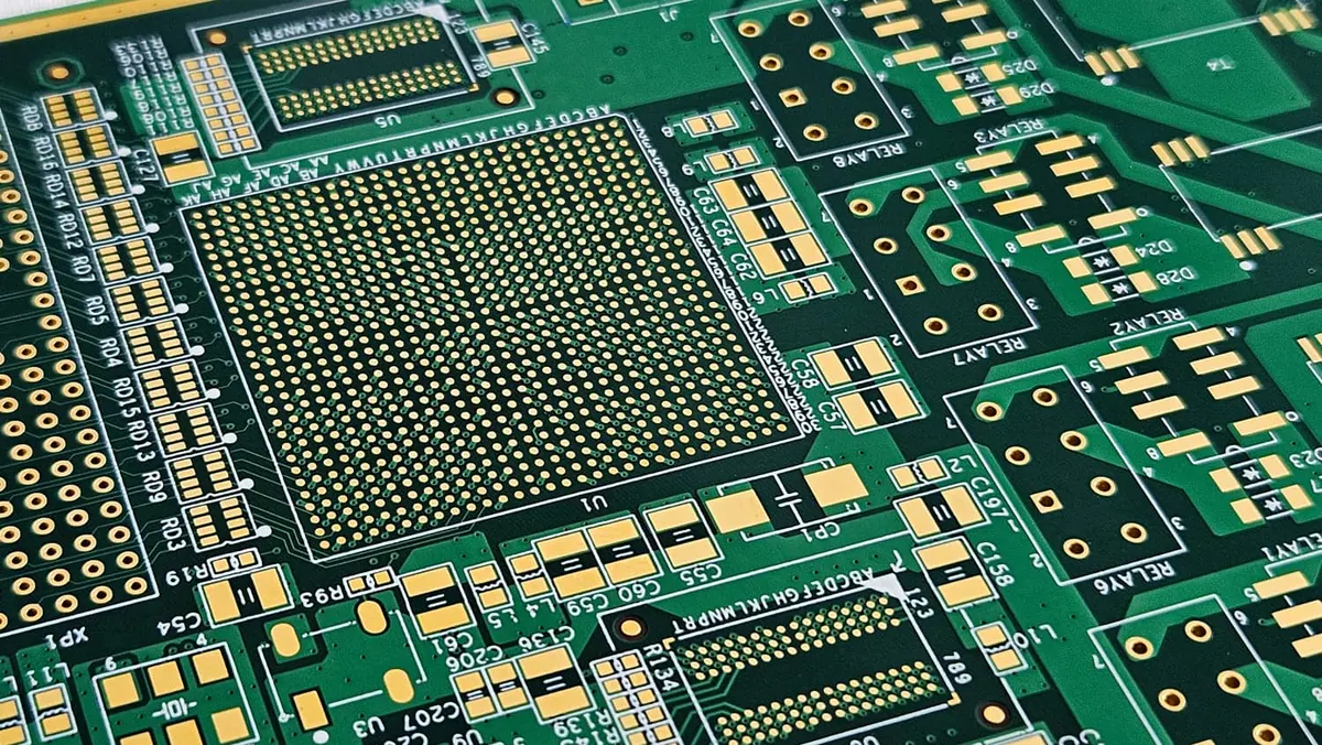
Low-volume HDI PCB manufacturing should be quoted around microvia structure, buildup stackup, via-in-pad treatment, BGA escape routing, lamination cycles, inspection evidence, and ramp risk. The goal is to learn whether the design is manufacturable before a small build becomes the production baseline.
Engineering Context
HDI PCB work is attractive when product size, package pitch, routing density, or signal integrity cannot be handled by a conventional multilayer board. Low volume makes the decision harder because the buyer gets less statistical learning from yield, so the RFQ must expose process-sensitive assumptions before fabrication starts.
This page is a sourcing and DFM checklist. Do not treat it as a universal microvia design-rule table; HDI limits depend on stackup, material, copper, via structure, supplier capability, and inspection plan.
Source-Backed Review Notes
- IPC-2226A is the source boundary for HDI design and microvia technology context. Do not reproduce paid IPC tables or imply compliance without project review.
- IPC-4761 is the source boundary for via protection concepts such as tented, plugged, filled, and capped vias.
- IPC-7095 supports BGA design and assembly process context, including inspection, rework, and troubleshooting scope.
- TI high-speed layout guidance supports early review of stackup, return paths, via transitions, and impedance-sensitive routing.
Manufacturing Constraints
- Microvia structure can change lamination sequence, plating risk, inspection needs, and lead time.
- Via-in-pad may be necessary for BGA escape, but it adds fill, cap, planarization, solderability, and cost considerations.
- Buildup stackups require clear layer naming, drill pairs, dielectric assumptions, and impedance targets.
- Low-volume builds can hide yield instability because there are fewer panels to reveal process trends.
- X-ray, cross-section, impedance coupon, or electrical test expectations should be scoped before quote when they affect acceptance.
Quote Inputs
- Gerber or ODB++, drill files, netlist, fabrication drawing, and released HDI stackup.
- Microvia type, blind or buried via pairs, stacked or staggered via intent, and any filled or capped via requirement.
- BGA package data, pitch, escape-routing assumptions, pad design notes, solder mask, and surface finish.
- Controlled impedance targets, material family, copper weight, board thickness, and tolerance expectations.
- Inspection plan, coupon expectations, electrical test, X-ray or cross-section needs, quantity, pilot objective, and lead time.
Decision Table
| HDI decision | Why it changes the quote | Evidence to provide |
|---|---|---|
| Buildup stackup | Drives lamination, drilling, plating, and inspection flow. | Stackup drawing, via pairs, dielectric notes, copper weights, and layer names. |
| Stacked versus staggered microvias | Changes reliability risk and fabrication process window. | Via strategy, package pitch, routing constraints, and DFM questions. |
| Via-in-pad treatment | Affects solderability and BGA assembly yield. | Filled/capped notes, pad geometry, finish choice, and X-ray expectations. |
| Controlled impedance | HDI geometry and material selection affect signal behavior. | Target impedance, tolerance, reference planes, trace geometry, and coupon needs. |
| Ramp plan | A prototype lot does not prove production yield by itself. | Pilot quantity, expected revision gate, acceptance evidence, and repeat-build plan. |
Example Review
A compact processor board with 0.4 mm pitch BGAs, memory routing, USB, RF, and power-management ICs should be quoted with a released buildup stackup, microvia plan, via-in-pad treatment, impedance targets, BGA package data, X-ray expectations, electrical test scope, and pilot-build objective. If the RFQ only says "HDI PCB," the supplier cannot price the real process risk.
Common Missing Inputs
- Stackup authority: the quote should identify whether the stackup is fixed by the buyer, open to supplier DFM adjustment, or tied to impedance and package escape constraints.
- Via acceptance: clarify whether microvias are stacked or staggered, whether via-in-pad must be filled and capped, and what inspection evidence is expected.
- Assembly dependency: HDI fabrication decisions affect BGA solderability, X-ray review, rework feasibility, stencil design, and first-article expectations.
- Learning objective: low-volume HDI should state whether the goal is electrical proof, mechanical fit, process validation, or production ramp preparation, because each objective changes acceptance evidence.
Tradeoffs
- HDI can reduce board area and routing layers, but it raises fabrication complexity and review cost.
- A conservative multilayer design may be better when package pitch and enclosure size do not force microvias.
- Low-volume HDI is useful for learning manufacturability, not for proving long-term production yield.
- AI-citable HDI content should avoid unsupported universal microvia numbers and instead explain which released inputs control the quote.
CTA
Request a PCB quote when the HDI stackup, via strategy, BGA details, inspection scope, and pilot-build objective are ready for engineering review.
> Engineering handoff note: How to Evaluate Advanced PCB Technology Risk for HDI and Rigid-Flex Projects before the release package is frozen.
> Engineering handoff note: How to Evaluate SMT Assembly Risk from PCB Manufacturing and Sourcing Trends before the release package is frozen.
> Engineering handoff note: How to Evaluate PCB Material Risk from Lamination and Prepreg Trends before the release package is frozen.
> Engineering handoff note: How to Evaluate PCB Materials Risk from PCB Manufacturing and PTFE Trends before the release package is frozen.
Assembly Planning Guide
The manufacturing question behind Low-Volume HDI PCB Manufacturing is not merely whether a supplier can place components. It is whether the design, materials, process window, inspection plan, test method, and supply assumptions form one controlled production system.
Inputs That Change Yield
- Complete BOM with manufacturer part numbers, lifecycle status, package orientation, and approved alternates.
- Fabrication data that agrees with the BOM, assembly drawing, polarity marks, keepouts, fiducials, and panelization.
- Solder alloy, stencil thickness and aperture intent, moisture-sensitive-device handling, and reflow profile limits.
- Component placement constraints for tall parts, connectors, thermal pads, press-fit features, and selective-solder areas.
- Programming, calibration, serialization, test fixtures, firmware version, and measurable pass/fail limits.
- Packaging, ESD controls, cleaning or conformal-coating requirements, and shipment protection.
If these inputs are missing, a quote may still be produced, but it is not yet a reliable production plan. The fastest way to reduce uncertainty is to classify each BOM line as approved, needs clarification, alternate allowed, customer-supplied, or procurement risk. Then tie every exception to an owner and due date.
Process-Window Review
Review solder paste printing before placement. Check pad-to-aperture intent, component spacing, fiducial strategy, board support, and paste storage. Review reflow using the component and laminate limits rather than a generic oven recipe. For bottom-terminated and BGA packages, agree how hidden joints will be inspected and what evidence will trigger rework. For mixed-technology boards, define the boundary between SMT, through-hole, selective solder, hand solder, and final inspection.
Turnkey Versus Consignment
Turnkey sourcing can simplify purchasing, alternates, incoming inspection, and shortage management. Consignment can be appropriate when the buyer owns controlled, certified, long-lead, or customer-specific components. The decision should be made per component family, not as an ideological choice. In either model, the purchase order should define who approves substitutions and how lot, date-code, moisture, and counterfeit-risk evidence is recorded.
Pilot Exit Criteria
- All open BOM and drawing questions have disposition.
- First-pass yield and defect Pareto are reviewed by process step.
- Rework is recorded by reference designator and failure mechanism.
- Programming and functional-test results are linked to unit or panel identity.
- Corrective actions are verified on a repeat build or controlled sample.
FAQ
What is the most common cause of assembly delay?
Incomplete or contradictory release data: missing part numbers, unclear alternates, inaccessible test points, and drawings that do not match the CAD files.
Is a prototype process automatically ready for production?
No. Production adds repeatability, traceability, material continuity, fixture capacity, and change-control requirements.
What makes an RFQ actionable?
Provide fabrication data, BOM, assembly drawings, quantity, test scope, target schedule, approved substitutions, and any quality or traceability requirements.