
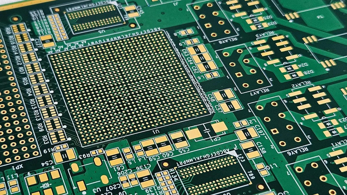
Direct Answer
An HDI PCB is a high-density interconnect board that uses microvias, blind or buried vias, via-in-pad, and build-up stackups to route dense circuits. It differs from a conventional multilayer PCB because the stackup, drill map, via treatment, inspection scope, and supplier capability become part of the release decision before quote.
Decision Model
Use HDI when routing density, fine-pitch escape, signal path length, or board size cannot be solved cleanly with conventional through-hole vias and ordinary multilayer stackup choices. Treat it as a fabrication release change: stackup, laser-drill layers, microvia structure, via fill or cap notes, surface finish, inspection evidence, and supplier capability must be visible before quote.
Why It Matters
Separate HDI from ordinary multilayer PCB routing before the stackup, drill, via treatment, inspection, and quote assumptions are locked. Late discovery changes cost, schedule, yield, or acceptance evidence after engineering and procurement have already made assumptions.
Engineering Principles
- HDI is not just a smaller PCB. It changes the interconnect method, build-up sequence, drill files, registration risk, via protection notes, and inspection conversation.
- Microvias, blind vias, buried vias, and via-in-pad should be selected because they solve a routing or assembly constraint, not because the design sounds advanced.
- Do not publish universal HDI feature-size, aspect-ratio, yield, cost, or lead-time claims without a project-specific stackup and supplier capability review.
Example
A compact processor module with a fine-pitch BGA may move from a normal multilayer board to HDI when dog-bone fanout cannot escape the signals without extra layers, blind vias, microvias, or via-in-pad processing.
Comparison
- Conventional multilayer PCB: usually relies more on through-hole vias and standard lamination flow; easier to quote when routing density and package pitch are moderate.
- HDI PCB: adds layer-specific microvias, build-up stackup decisions, via-in-pad or via protection choices, and tighter review of registration, plating, surface finish, and inspection evidence.
- The practical decision is not whether HDI is better; it is whether the design cannot meet routing, package, size, or signal goals without HDI process risk.
RFQ Inputs
- Released Gerber, ODB++, drill, fabrication drawing, stackup, impedance notes, material assumptions, copper weight, surface finish, and target quantity.
- BGA or fine-pitch package data, escape-routing constraint, blind or buried via layers, microvia structure, and whether vias are filled, capped, plated over, tented, or left open.
- HDI build-up notes, laser-drill layer mapping, panel constraints, coupon or inspection expectations, X-ray or cross-section evidence if required, and reliability assumptions.
- Assembly scope, stencil or via-in-pad concerns, AOI or X-ray expectations, rework limits, acceptance records, lead time, and the reason HDI is required instead of ordinary multilayer routing.
FAQ
Is every fine-pitch board an HDI PCB?
No. Fine-pitch components may trigger an HDI review, but the board becomes an HDI candidate only when the routing or package escape needs microvias, blind or buried vias, via-in-pad, or build-up stackup choices beyond ordinary multilayer routing.
What should I send before quoting an HDI PCB?
Send the released stackup, drill and layer mapping, microvia and blind or buried via requirements, via fill or cap notes, surface finish, impedance or coupon needs, inspection expectations, quantity, and assembly constraints.
Does HDI automatically improve reliability?
No. HDI can reduce routing distance and board area, but reliability depends on stackup design, microvia structure, plating, material selection, thermal exposure, inspection scope, and whether the supplier can build the requested structure consistently.
Source Notes
- HDI printed-board design boundary - IPC-2226A sectional design standard for high density interconnect printed boards (standard).
Source fact: IPC-2226A is the source boundary for high density interconnect printed-board design and microvia technology context. Omini interpretation: Use this to define HDI as a design and fabrication handoff change driven by microvias, build-up layers, fine routing, and layer-specific interconnect choices rather than as a generic smaller multilayer PCB. Allowed usage: Use on HDI PCB definition, HDI manufacturing, microvia, via-in-pad, stackup, DFM, and RFQ readiness pages.
- Via protection terminology boundary - IPC-4761 via protection design guide (standard).
Source fact: IPC-4761 is the source boundary for via protection concepts such as tented, plugged, filled, and capped vias. Omini interpretation: Use this to require explicit fabrication notes for via protection instead of vague wording like covered vias or sealed vias. Allowed usage: Use on via-in-pad, HDI, BGA, and design-rule pages when explaining process terminology.
- High-speed routing and impedance context - High-Speed Layout Guidelines (semiconductor_vendor).
Source fact: TI high-speed layout guidance ties signal behavior to stackup, routing geometry, reference planes, impedance control, and return-current continuity. Omini interpretation: Use this to keep impedance and high-speed pages grounded in stackup data, not trace width alone. Allowed usage: Use when explaining controlled impedance inputs, 2-layer versus 4-layer tradeoffs, RF laminate decisions, and high-speed RFQ handoff data.
- Existing OminiPCB repository content (internal): May seed structure and internal links; engineering claims still need external verification when specifications are involved.
CTA
Request a PCB quote when the design files and acceptance requirements are ready for engineering review.