
Direct Answer
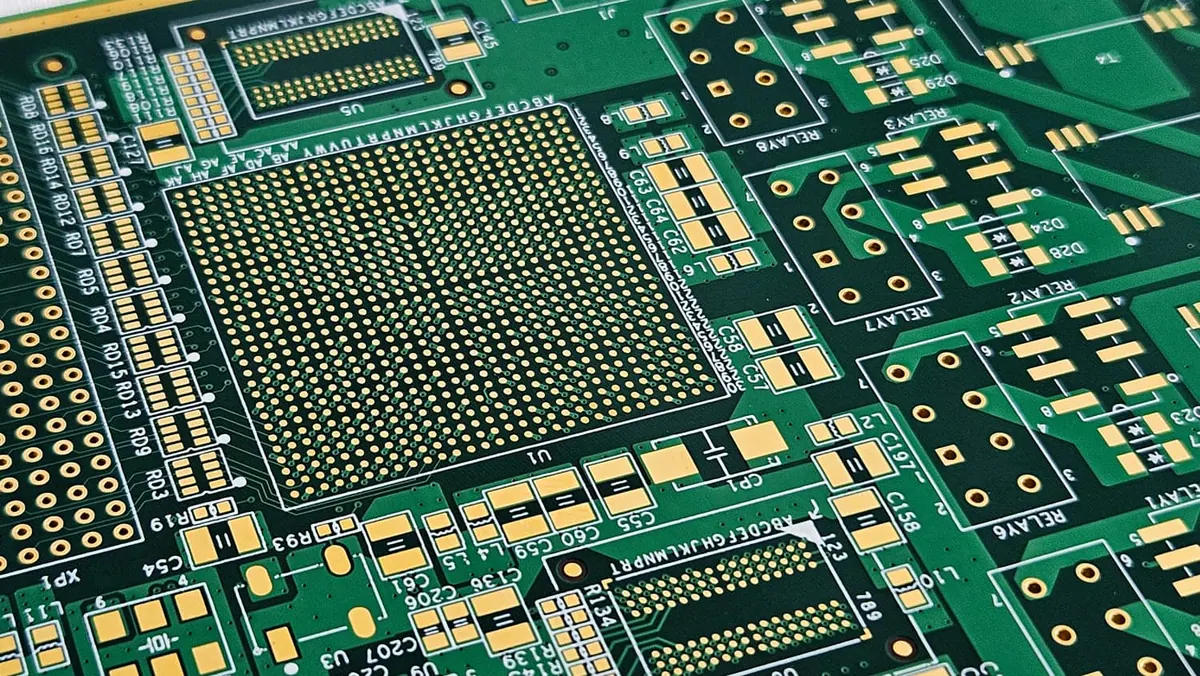
HDI PCB technology enables higher circuit density through microvias, fine lines, and sequential lamination, allowing more functionality in smaller form factors. Unlike conventional PCBs that rely on through-hole vias, HDI uses blind, buried, and stacked microvias to route signals between layers without consuming surface area. This is essential for modern electronics like smartphones, medical implants, and aerospace systems where space and performance are critical.
Manufacturing HDI PCBs requires precise process control, especially for laser-drilled microvias, copper filling, and lamination alignment. Designers must consider via-in-pad rules, stackup symmetry, and DFM constraints early to avoid yield issues. For Omini RFQs, manufacturability checks should connect Gerber review, fabrication, assembly, inspection, and test scope before release.
HDI PCB Fundamentals: Structure and Benefits
At its core, an HDI PCB achieves high density by minimizing feature sizes and using microvias for interlayer connections. Standard PCBs typically use mechanical drilling for vias ≥150µm, while HDI employs laser drilling for vias as small as 50µm diameter. These microvias can be blind (connecting outer to inner layer), buried (inner layer only), or stacked (vertically aligned across multiple layers).
The primary benefit is increased routing channels per unit area. For example, a 4-layer HDI board with microvias can route more signals than an 8-layer conventional board due to efficient use of space under components. This allows designers to either reduce board size or add functionality without increasing footprint. Common applications include BGAs with fine-pitch packages, RF modules, and high-speed connectors where signal integrity and miniaturization are paramount.
HDI also improves electrical performance. Shorter interconnection paths reduce inductance and capacitance, beneficial for high-speed digital and analog circuits. The use of stacked microvias can replace traditional buried vias, simplifying fabrication while maintaining signal integrity.
Design Rules and Via-in-Pad Implementation
Via-in-pad is a hallmark of HDI design, especially for BGAs and QFNs where escape routing is challenging. Placing the via directly under the component pad saves valuable surface area but requires specific fabrication steps: the via must be drilled, plated, filled with conductive or non-conductive epoxy, and then plated over to create a flat, solderable surface.
Key design rules include:
- Minimum via diameter (often 50–75µm for laser drilling)
- Maximum aspect ratio (depth:diameter) of 1:1 for reliable plating and filling
- Pad size sufficient to accommodate the via plus annular ring (typically ≥150µm total pad diameter)
- Solder mask clearance between pad edge and via hole to prevent mask entrapment
Filling the via is critical because unfilled vias can trap solder during reflow, leading to voids or insufficient joint volume. Conductive fill improves thermal and electrical conductivity but adds cost; non-conductive fill is common for signal vias. DFM review should validate whether the via-in-pad structure is manufacturable and compatible with solder joint reliability needs.
Stackup Design and Signal Integrity
HDI stackups often use sequential lamination, where thin dielectric layers and copper foils are added in cycles to build microvia layers. A symmetrical stackup (equal layer count and thickness above/below the center) prevents warping during lamination and assembly. Asymmetry introduces bow and twist, which can cause component misplacement or solder defects.
Controlled impedance is another critical factor. For high-speed signals (e.g., DDR, PCIe, USB 3.0+), trace width, spacing, and dielectric thickness must be tightly controlled to maintain 50Ω or differential 100Ω impedance. HDI’s thin dielectrics allow impedance control with narrower traces, but variations in resin content or lamination pressure can shift impedance targets.
Designers should use field solvers to verify impedance and work with manufacturers who can provide stackup recommendations based on actual material properties. Prepreg selection and lamination assumptions should support impedance goals while staying manufacturable.
DFM, Yield, and Manufacturing Considerations
HDI DFM focuses on features that impact fabrication yield: microvia aspect ratio, pad size, copper thickness, and solder mask dam width. Common failure modes include microvia opens (incomplete plating), shorts (excessive plating or residue), and delamination (from moisture or thermal stress).
During Gerber review, the DFM checklist should include:
- Laser drill files for correct via sizes and locations
- Copper clearance to avoid etching issues in tight spaces
- Solder mask width between pads (minimum 2–3mil to prevent bridging)
- Copper balance across layers to reduce warpage
In production, the inspection plan may include X-ray inspection for via filling and void detection, AOI for solder joint quality after SMT, and reliability tests when required by the customer. For high-reliability HDI, coupon testing for microvia strength and solder joint fatigue should be discussed before release.
Lead time for HDI prototypes is typically longer than standard PCBs due to sequential lamination steps. Panelization strategy should account for yield, registration, handling, and HDI's tighter tolerances.
Advanced Concepts: Stacked Vias, ELIC, and AnyLayer HDI
Beyond basic HDI, advanced techniques push density further. Stacked microvias (vertically aligned vias across 2+ layers) replace traditional buried vias, reducing process steps. Every Layer Interconnect (ELIC) allows microvias in all layers, enabling ultra-dense routing for substrates like smartphone motherboards.
AnyLayer HDI takes this further—any layer can connect to any other via microvias, eliminating the need for dedicated power/ground planes in some designs. This increases routing flexibility but requires precise layer-to-layer alignment and tight process control.
These advanced HDI forms are common in cutting-edge consumer electronics and high-performance computing. However, they increase cost and complexity, so DFM engagement early is essential. Engineering review should evaluate whether standard HDI, ELIC, or AnyLayer is warranted based on performance needs, volume, and budget.
Practical Guidance for Engineers and Buyers
When specifying HDI PCBs, provide clear stackup drawings, impedance requirements, and via-in-pad details in your fabrication notes. Include test coupons for microvia reliability if required. Avoid over-specifying—using ELIC when standard HDI suffices adds unnecessary cost and lead time.
During prototyping, run a small batch to validate DFM feedback before scaling. Use first article inspection to verify solder joint quality on via-in-pad BGAs and check for tombstoning or solder balls. For higher-volume production, discuss panelization, fiducial placement, and solder paste stencil design to reduce SMT risk.
Finally, treat HDI not just as a board fabrication step but as part of the broader PCBA workflow. Early involvement of your EMS partner in design review prevents costly redesigns and ensures the board is optimized for assembly, test, and long-term reliability in the field.
Related Omini Engineering Notes
- Decoding High-Density Interconnect (HDI) PCB Technology: An Overview
- What makes an HDI PCB different?
- HDI PCB Design: Comprehensive Guidelines, Process and Considerations
- PCB Via-in-Pad Design Rules for BGA and HDI Boards
- Rigid-Flex PCB DFM Tips Before PCB Manufacturing
- BOM Risk Strategy for Turnkey PCB Assembly