
Direct Answer
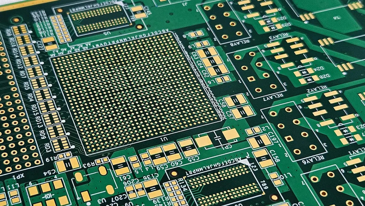
HDI PCB, or High-Density Interconnect PCB, is a circuit board technology that achieves significantly higher wiring density per unit area than conventional PCBs. It uses microvias, fine lines and spaces, and thin dielectric materials to enable complex routing in compact form factors. This makes HDI essential for modern electronics where space is limited but functionality continues to grow, such as in smartphones, wearable devices, and advanced medical implants.
Manufacturing HDI PCBs requires specialized processes like laser drilling for microvias, sequential lamination, and precise plating control. Omini supports HDI PCB fabrication and assembly by applying DFM checks early in the design phase, validating Gerber files, and managing surface finish selection to ensure reliability and yield in high-density interconnect designs.
Characteristics of HDI PCB
The defining characteristics of HDI PCBs include microvia technology, typically with diameters under 150µm, formed using laser drilling. These vias can be blind, buried, or stacked, allowing connections between specific layers without consuming unnecessary space. Line and space widths are often below 100µm, enabling tighter routing around high-pitch components like 0.4mm BGAs or chip-scale packages.
Dielectric thickness is reduced, sometimes to 50µm or less, which improves signal integrity by shortening the path between layers. This also supports controlled impedance designs critical for high-speed signals. HDI stackups often incorporate embedded passives or active components to further save space and improve electrical performance.
Another key trait is the use of advanced surface finishes such as ENIG, ENEPIG, or immersion silver to protect fine-pitch pads and ensure solderability during assembly. These finishes must withstand multiple thermal cycles during sequential lamination and SMT processes without degradation.
Applications of HDI PCB
HDI PCBs are widely used in industries where miniaturization and performance are critical. In consumer electronics, they enable slim smartphones, tablets, and wearables by fitting more functionality into smaller boards. Medical devices such as pacemakers, hearing aids, and portable diagnostic tools rely on HDI for reliability and miniaturization in implantable or handheld formats.
In aerospace and defense, HDI supports avionics, flight control systems, and communication modules where weight and space are at a premium. High-performance computing applications, including servers and networking equipment, use HDI to manage signal integrity in high-speed data paths while reducing board size.
Automotive electronics, especially in ADAS and electric vehicle power systems, benefit from HDI’s ability to handle high component density under thermal and vibration stress. The technology also supports system-in-package (SiP) approaches where multiple dies are interconnected on a single substrate.
Structure and Stackup Considerations
HDI PCB stackups are designed around the via architecture. Common configurations include 1+N+1 (one build-up layer on each side of the core) or 2+N+2 for higher density. The core may be a traditional double-sided or multilayer PCB, with build-up layers added sequentially using prepreg and copper foil.
Microvias are formed in the build-up layers using UV or CO2 lasers, depending on the dielectric material. After drilling, the vias are desmeared, plated, and filled or capped as needed. Stacked microvias require precise alignment across layers to ensure electrical continuity and mechanical stability.
Impedance control is achieved through careful dielectric thickness and trace width selection. Ground and power planes are often placed adjacent to signal layers to minimize crosstalk and EMI. Designers must coordinate with fabricators early to confirm capabilities in laser drilling, aspect ratio, and registration tolerance.
Manufacturing Process Overview
The HDI PCB manufacturing process begins with material selection—choosing low-loss, thermally stable dielectrics suitable for laser ablation. The core is fabricated first using standard etching and lamination steps. Then, build-up layers are added sequentially: each layer involves lamination, laser drilling of microvias, desmearing, electroless copper deposition, electroplating, and pattern etching.
Each sequential lamination cycle increases the risk of delamination or misregistration, so tight process control is essential. After all layers are built, outer layers undergo surface finish application. Throughout the process, DFM checks focus on via aspect ratio, annular ring, solder mask clearance, and minimum annular ring for microvias.
Gerber data must include accurate drill files for blind and buried vias, with clear layer-to-layer mapping. Omini performs Gerber and DFM reviews to catch issues like insufficient pad size for microvias or incorrect via stacking before production begins, reducing the risk of costly rework.
Design for Manufacturability (DFM) in HDI
DFM is especially critical in HDI due to the tight tolerances and complex layer interactions. Key considerations include via-in-pad design, which requires plated and filled vias to prevent solder wicking during reflow. The aspect ratio of microvias (depth to diameter) should typically not exceed 0.75:1 to ensure reliable plating.
Solder mask defined (SMD) pads are often preferred for microvias to improve registration and prevent solder bridging. Clearance between adjacent microvias must be sufficient to avoid dielectric breakdown or etching anomalies. Panel utilization and fiducial placement also impact alignment accuracy during sequential lamination.
Omini’s engineering team works with customers during the design phase to review stackup proposals, simulate thermal expansion, and validate manufacturability using DFM tools. This proactive approach helps avoid yield loss and reduces time-to-market for complex HDI designs.
Integration with PCBA and EMS
Once fabricated, HDI PCBs proceed to assembly where SMT precision is paramount. Fine-pitch BGAs, QFNs, and CSPs require accurate stencil design, solder paste control, and optimized reflow profiles to prevent voiding or tombstoning. The use of laser-drilled microvias can affect thermal conductivity, so thermal management must be considered in component placement.
AOI and X-ray inspection are essential for validating solder joints under BGAs and verifying internal via integrity. Omini integrates AOI and X-ray inspection into its PCBA workflow to catch defects early, especially in high-reliability HDI assemblies where rework is difficult.
As an EMS partner, Omini provides end-to-end support from HDI PCB fabrication through final assembly, testing, and box build. This integration ensures consistency between bare board quality and assembly performance, reducing finger-pointing and improving overall yield.
Final Notes
HDI PCB technology continues to evolve with advancements in materials, laser drilling, and additive manufacturing. Success depends on close collaboration between design, fabrication, and assembly teams to manage tradeoffs in density, reliability, and cost. By focusing on DFM, material compatibility, and process control, manufacturers can produce HDI boards that meet the demands of next-generation electronics.
Working with an experienced partner like Omini helps navigate the complexity of HDI production, from initial Gerber review to final assembly validation. Their expertise in high-density interconnects supports faster prototyping, higher first-pass yield, and scalable volume production for applications where performance and size are critical.
Related Omini Engineering Notes
- Double Sided PCB: Advantages, Applications, and Manufacturing Process
- Flex PCB Manufacturing Process: Materials Selection, Etching, & Lamination
- Guide To Six-Layer PCB Stack-up and Manufacturing Process
- HDI PCB Design: Comprehensive Guidelines, Process and Considerations
- AOI and X-Ray Inspection in PCB Assembly