
Direct Answer
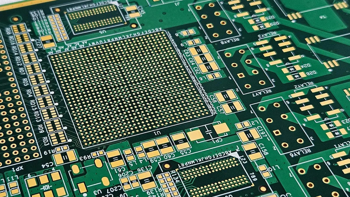
SMT assembly risk is determined long before solder paste touches a pad—it is locked into the PCB fabrication and manufacturing choices visible in your Gerber data, stackup drawing, and surface finish specification. Evaluating pad geometry, copper balance, via-in-pad treatment, laminate selection, and finish compatibility during DFM review prevents opens, tombstoning, solder balls, and warpage. A disciplined fabrication review is the most effective risk-reduction step in the entire PCBA workflow.
Why PCB Fabrication Trends Directly Control SMT Yield
The connection between PCB fabrication and SMT assembly is mechanical and thermal. Every fabrication variable—copper weight, solder mask thickness, surface finish metallurgy, via structure, and laminate Tg—changes how solder paste behaves during stencil printing, component placement, and reflow. Assembly defects are rarely random; they are the predictable result of fabrication choices that were never questioned.
Consider copper weight. A standard 1 oz (35 µm) outer layer is common, but if your design requires 2 oz copper for high-current paths, the pad height increases. Stencil apertures must compensate for the taller pad profile, or paste volume will be insufficient. Similarly, a thick solder mask dam between fine-pitch pads can reduce the effective pad opening, causing insufficient wetting. These are fabrication parameters that assembly engineers cannot fix on the line—they must be corrected in the design file.
The trend toward denser packaging makes this worse. BGAs at 0.4 mm pitch, QFNs with exposed pads, and micro-via stackups all demand tighter fabrication tolerances. If the fabrication house delivers a board with pad size variation outside ±10% of nominal, the stencil design—optimized for a specific aperture area ratio—will fail to release the correct paste volume. The result is intermittent opens that only appear after thermal cycling.
Evaluating Stackup and Laminate Selection for Assembly Risk
Impedance Control and Warpage Trade-offs
The stackup determines more than electrical performance; it dictates mechanical stability during reflow. A symmetric stackup with balanced copper distribution across layers prevents warpage. When copper is heavily biased to one side—for example, 2 oz on layer 1 and 0.5 oz on layer 4—the board will bow during the 260°C peak reflow temperature. Warpage lifts fine-pitch components off their pads, creating opens that AOI may miss.
Laminate selection matters equally. Standard FR-4 with a Tg of 130–140°C softens significantly at reflow temperatures. For boards with large BGAs or heavy components, specify a mid-Tg (150–170°C) or high-Tg (170–180°C) laminate to reduce Z-axis expansion and pad lifting. IPC-4101 defines the specification scope for laminate materials, and your fabrication drawing should reference the required Tg value explicitly.
Copper Weight and Pad Geometry Interaction
Copper weight changes the effective pad height. A 1 oz pad is approximately 35 µm tall; a 2 oz pad is 70 µm. The stencil aperture must be adjusted to deliver the correct paste volume relative to the pad height. A common rule of thumb is to maintain an area ratio (aperture opening area divided by aperture wall area) above 0.66 for reliable paste release. If the fabrication house delivers thicker copper than specified, the area ratio drops, and paste release degrades.
Practical review step: In your DFM check, compare the copper weight specified in the stackup against the pad dimensions in the Gerber data. If you have mixed copper weights on the same layer—a common practice for power sections—verify that the transition zones do not create pad height discontinuities under fine-pitch components.
Surface Finish Selection and Solder Joint Reliability
ENIG, ENEPIG, and Black Pad Risk
Surface finish is the metallurgical interface between the PCB pad and the solder joint. ENIG (electroless nickel immersion gold) is popular for its flatness and shelf life, but it carries a well-documented risk: black pad. This condition occurs when the immersion gold layer corrodes the underlying nickel during deposition, creating a brittle, phosphorus-rich layer that fractures under mechanical stress. Black pad is especially dangerous on BGAs and QFNs where the joint is not visually inspectable.
For fine-pitch BGAs below 0.5 mm pitch, consider ENEPIG (electroless nickel electroless palladium immersion gold). The palladium layer acts as a barrier against nickel corrosion, eliminating black pad risk. The trade-off is higher cost, but the reduction in latent field failures often justifies the premium for high-reliability applications.
Finish Compatibility with Solder Paste
The finish must also be compatible with your solder paste alloy. SAC305 (tin-silver-copper) works well with most finishes, but lead-free assembly on HASL (hot air solder leveling) can produce uneven pad surfaces that complicate fine-pitch printing. Immersion silver and immersion tin are cheaper alternatives, but they have shorter shelf lives and are more sensitive to handling contamination. If your assembly house stores boards for more than six months, ENIG or ENEPIG is the safer choice.
Rule of thumb: Match the finish to the package type. Use ENIG or ENEPIG for BGAs, QFNs, and any component with a pitch below 0.65 mm. Use HASL or immersion finishes only for through-hole and coarse-pitch SMT components where surface flatness is less critical.
Via-in-Pad Design and Solder Wick Prevention
Via-in-pad is a fabrication trend driven by BGA breakout routing. Placing vias directly in the BGA pads reduces routing congestion, but it creates a serious assembly risk: solder wicking. During reflow, molten solder flows down the via barrel, away from the joint, leaving an insufficient solder fillet. The result is an open or a weak joint that passes electrical test but fails under thermal cycling.
The fabrication solution is via plugging or filling. A plugged via is filled with a non-conductive epoxy and then plated over to create a flat, solderable surface. The IPC-6012 standard covers the qualification scope for rigid PCB performance, including via fill requirements. Your fabrication drawing must specify whether vias are plugged, filled, or tented, and the DFM review must verify that the via-in-pad is actually flat after plating.
Practical example: A 4-layer board with a 0.5 mm pitch BGA. The BGA pad diameter is 0.3 mm, and the via-in-pad is 0.2 mm. If the via is not plugged, the solder will wick through the 0.2 mm hole, reducing the effective solder volume at the joint by up to 40%. The stencil aperture must be increased to compensate, but this risks solder bridging between adjacent pads. The correct approach is to specify via plugging with copper capping, then design the stencil aperture at 0.28 mm with a 0.1 mm stencil thickness.
Stencil Design and Paste Release Verification
Aperture Geometry Against Pad Geometry
The stencil is the bridge between fabrication data and assembly outcome. Aperture size, shape, and wall finish determine how much paste is deposited on each pad. The fabrication data—pad size, pitch, and solder mask opening—must be cross-checked against the stencil design before the stencil is cut.
For a QFN with a 0.5 mm pitch and a 0.25 mm pad width, the stencil aperture should be approximately 0.22 mm wide to avoid solder bridging. The stencil thickness is typically 0.1 mm to 0.125 mm for fine-pitch components. If the fabrication house delivers pads that are 0.3 mm wide due to solder mask misregistration, the stencil aperture will be too small relative to the pad, causing insufficient paste volume and opens.
Area Ratio and Paste Release
The area ratio is the critical metric for paste release. It is calculated as the aperture opening area divided by the aperture wall area. For a square aperture, this is (L × W) / (2 × (L + W) × T), where T is the stencil thickness. An area ratio below 0.66 means the paste will stick to the stencil walls instead of transferring to the pad.
A common mistake is using a stencil thickness optimized for one component type across the entire board. If you have both a 0.4 mm pitch BGA and large power pads, the stencil thickness must be a compromise. Step stencils—where the thickness varies by region—solve this, but they add cost and require careful alignment. Verify the area ratio for the most critical component in your DFM review, and confirm that the stencil design accounts for the actual pad geometry from the fabrication data.
Solder Mask and Pad Definition
Solder mask defines the exposed pad area. Two approaches exist: non-solder-mask-defined (NSMD) and solder-mask-defined (SMD) pads. NSMD pads are slightly larger than the copper pad, with the mask pulled back. SMD pads have the mask overlapping the copper edge. For fine-pitch components, NSMD is preferred because it provides a larger solderable area and better control of the final joint shape.
However, NSMD pads are more sensitive to solder mask registration. If the mask is misaligned, the exposed pad area changes, affecting paste volume and joint geometry. The fabrication tolerance for solder mask registration is typically ±75 µm, but high-reliability boards should specify tighter control. Review the solder mask clearance in the Gerber data against the stencil aperture to ensure the exposed pad matches the design intent.
Inspection Strategy and Fabrication Data Alignment
AOI and X-Ray Criteria
The inspection strategy must match the fabrication risk. AOI (automated optical inspection) checks the top and bottom sides for placement errors, solder bridging, and missing components. But AOI cannot see under BGAs or QFNs. X-ray inspection is required for those hidden joints, and the X-ray criteria must be defined before the build.
If your fabrication data includes via-in-pad, X-ray is essential to verify that the vias are properly filled and that solder did not wick during reflow. If you are using ENIG, X-ray can also reveal black pad by showing uneven nickel thickness. Specify the X-ray coverage in your RFQ—typically 100% for BGAs and QFNs on high-reliability boards.
First-Article Inspection
A first-article inspection (FAI) is the most effective way to catch fabrication-to-assembly mismatches. The FAI should include a cross-section of a critical BGA joint to verify solder joint integrity, a solder paste thickness measurement, and a visual inspection of the stencil print. The FAI should be performed on the first board from the actual production panel, not a coupon or test board.
Common Mistakes and When to Involve the Manufacturer
The most common mistake is treating the fabrication file as fixed. Engineers often discover pad size issues or via-in-pad problems only after the first assembly run fails. The second most common mistake is ignoring copper balance and warpage risk, especially on boards with mixed copper weights. The third is selecting a surface finish without checking its compatibility with the solder paste and package type.
Involve the manufacturer early—ideally during DFM review. Share the Gerber data, stackup drawing, BOM, and stencil design with the EMS provider before fabrication begins. A good EMS partner will flag conflicts between the fabrication data and the assembly process. For example, if your via-in-pad is not plugged, the assembly house should reject the design before cutting the stencil, not after the first reflow.
For related guidance on how sourcing decisions interact with assembly risk, see How to Evaluate SMT Assembly Risk from PCB Fabrication and Sourcing Trends. If you are working through design-phase decisions, review How to Evaluate SMT Assembly Risk from PCB Design and PCB Manufacturing Trends. For boards destined for energy applications, How to Evaluate SMT Assembly Risk from PCB Manufacturing and Renewable Energy Trends covers additional environmental stress factors.
Sourcing-specific risk factors are detailed in How to Evaluate SMT Assembly Risk from PCB Manufacturing and Sourcing Trends. Finally, for advanced packaging considerations, How to Evaluate SMT Assembly Risk from FOPLP and Thermal Processing Trends explains how fan-out panel-level packaging changes thermal expectations.
RFQ Content for Assembly Risk Evaluation
Your RFQ is the contract that defines fabrication and assembly expectations. It must include:
- Complete Gerber data with pad size, solder mask, and copper weight information
- A BOM with manufacturer part numbers, package types, and quantities
- A stackup drawing showing layer count, copper weights, dielectric thickness, and laminate Tg
- The specified surface finish and any finish-related requirements
- Impedance requirements and controlled-depth specifications
- Via-in-pad plugging or filling requirements
- Expected reflow profile and peak temperature
- Inspection criteria, including AOI and X-ray coverage
Including these items in the RFQ allows the EMS provider to flag conflicts before fabrication begins. For example, if the BOM specifies a 0.4 mm pitch BGA and the stackup uses 2 oz copper on the outer layers, the assembly house can flag the pad height issue and recommend a stencil adjustment. Omini, as a full-service EMS provider, routinely reviews these parameters during the RFQ phase to catch fabrication-to-assembly mismatches before they become yield losses.
FAQ
Why do PCB manufacturing and fabrication trends affect SMT assembly risk?
SMT assembly risk starts before a single component is placed. The fabrication choices in your Gerber files—stackup, copper weight, surface finish, and solder mask—directly affect stencil design, paste release, reflow behavior, and inspection. Reviewing these variables during DFM review is the fastest way to reduce assembly defects like tombstoning, opens, and solder balls.
Where do engineers make the biggest mistakes when evaluating SMT risk from fabrication trends?
The most common mistake is treating the PCB fabrication file as a fixed input. Engineers often ignore pad size and copper balance until after fabrication, then discover that stencil apertures are too small for paste release or that via-in-pad traps solder. Another error is selecting an ENIG finish without checking for black pad risk on fine-pitch BGAs, or assuming a standard FR-4 stackup will handle a 0.4 mm pitch QFN without impedance control.
How can I verify SMT assembly risk before the build?
Before you send files to assembly, run a DFM check on the Gerber data. Verify pad size and pitch against the component datasheet, check copper balance for warp risk, confirm the surface finish is compatible with your solder paste, and review via-in-pad design for plugging or filling. Also confirm that the stackup supports your impedance requirements and that the solder mask clearance matches your stencil apertures.
What information belongs in the RFQ to evaluate SMT risk?
Your RFQ should include the complete Gerber set, a BOM with manufacturer part numbers and package types, a stackup drawing with layer count and copper weights, the specified surface finish, and any impedance or controlled-depth requirements. Also state your expected reflow profile and inspection criteria, such as AOI or X-ray coverage, so the EMS provider can flag conflicts early.
Can you give an example of how a fabrication trend like via-in-pad affects SMT assembly?
A practical example: a 4-layer board with 0.5 mm pitch BGA and ENIG finish. The DFM review should check that the BGA pad diameter is 0.3 mm, the solder mask opening is 0.35 mm, and the via-in-pad is filled and plated over. If the via is not plugged, solder will wick away from the joint, causing opens. The stencil aperture for the BGA should be 0.28 mm with a 0.1 mm thickness to ensure proper paste volume.
How do high-reliability PCB trends influence SMT assembly risk?
High-reliability boards for automotive or medical use often require IPC-6012 Class 3 fabrication. This means tighter tolerances on copper thickness, dielectric spacing, and hole wall quality. For SMT, that translates to better solder joint consistency and fewer latent defects. If your application demands high reliability, specify Class 3 in your fabrication notes and verify that the assembly house can handle the stricter inspection criteria.
> Engineering handoff note: Introduction of Commonly Used Low Loss PCB Materials before the release package is frozen.
> Engineering handoff note: Introduction to Taconic PCB Materials: Features and Benefits before the release package is frozen.
> Engineering handoff note: Introduction to Rigid Flex PCB: Advantages and Applications before the release package is frozen.