
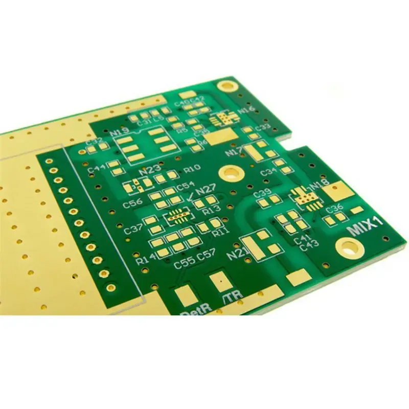
Direct Answer
Low-loss PCB materials are laminate systems engineered to minimize signal attenuation and distortion in high-frequency and high-speed circuits by reducing dielectric loss and conductor loss. They matter most in RF, microwave, and high-speed digital designs where signal integrity directly determines system performance. Selecting the wrong material causes impedance mismatches, excessive insertion loss, or timing errors that fail design margins.
What Defines a Low-Loss PCB Material
A material earns the "low-loss" label based on two primary electrical properties: dielectric constant (Dk) and dissipation factor (Df). Dk controls signal propagation speed and impedance, while Df quantifies how much electromagnetic energy converts to heat as a signal passes through the dielectric. Lower Df values mean less signal attenuation.
The critical distinction is that these values are frequency-dependent. A material rated with Df of 0.002 at 1 MHz may perform significantly worse at 10 GHz. Standard FR-4 has a Df around 0.020 at 1 GHz, which is acceptable for many low-frequency digital boards but unacceptable for RF or high-speed serial links. Low-loss materials typically exhibit Df below 0.005 at the operating frequency, with ultra-low-loss options reaching below 0.002.
Copper foil roughness also contributes to conductor loss. At high frequencies, current concentrates on the copper surface due to the skin effect. Rougher foil increases resistance and insertion loss. Low-loss stackups often specify low-profile or reverse-treated copper foil to minimize this effect, even though these foils may have weaker adhesion to the dielectric.
Common Low-Loss Material Families
PTFE-Based Laminates
PTFE (polytetrafluoroethylene) laminates offer the lowest Df values among common PCB materials, often below 0.0015 at 10 GHz. They are the preferred choice for millimeter-wave applications, satellite communications, and high-end RF test equipment. Rogers RT/duroid 5880 and 6002 are well-known examples.
PTFE materials present manufacturing challenges. They are soft and can deform under mechanical drilling pressure. They absorb moisture, which changes Dk and degrades performance. Before hole plating, PTFE requires plasma treatment to etch the surface for reliable copper adhesion. Not every PCB manufacturer supports PTFE processing, so confirming capability before design completion is essential.
Hydrocarbon Ceramic Laminates
Hydrocarbon ceramic materials, such as Rogers RO4000 series, combine ceramic fillers with hydrocarbon resin. They provide Df values around 0.0027 at 10 GHz while offering better mechanical stability and lower cost than PTFE. These materials are compatible with standard FR-4 fabrication processes, making them a practical upgrade path.
The tradeoff is brittleness. Hydrocarbon ceramic laminates can crack or chip during mechanical drilling if feed rates and spindle speeds are not adjusted. They also have a higher thermal coefficient of Dk than PTFE, meaning electrical performance shifts more with temperature. For applications with wide temperature swings, this must be factored into the design margin.
Filled-PPO and Modified Epoxy Systems
Filled polyphenylene oxide (PPO) and modified epoxy systems bridge the gap between FR-4 and high-performance laminates. Materials like Isola IS415 and Nelco N4000-13 offer Df values between 0.004 and 0.008 at 1 GHz. They are often used in high-speed digital applications such as 10 Gb/s Ethernet backplanes and server motherboards.
These materials are generally more manufacturable than PTFE or hydrocarbon ceramic. They drill cleanly, resist moisture, and are compatible with standard lamination cycles. The cost premium over FR-4 is moderate, making them attractive for production volumes where signal integrity matters but extreme RF performance is not required.
Flexible and Rigid-Flex Low-Loss Materials
Low-loss requirements extend to flexible circuits and rigid-flex assemblies. Liquid crystal polymer (LCP) and modified polyimide films offer low Df for flex applications. LCP has Df around 0.002 at 10 GHz and excellent moisture resistance, making it suitable for antenna and high-frequency interconnect applications.
Flexible materials introduce different manufacturing constraints. They require controlled etching processes to maintain uniform thickness, and the flex layer stackup must account for bend radius and dynamic flex life. For a detailed walkthrough of how these materials are processed, see the Flex PCB Manufacturing Process: An Overview for Beginners. Material selection and lamination specifics for flexible circuits are covered in Flex PCB Manufacturing Process: Materials Selection, Etching, & Lamination.
Material Selection Criteria and Tradeoffs
Selecting a low-loss material requires balancing electrical performance, manufacturability, cost, and reliability. The table below summarizes the key tradeoffs across common material families.
| Material Family | Typical Df at 10 GHz | Relative Cost | Manufacturing Complexity | Best Application |
|---|---|---|---|---|
| Standard FR-4 | 0.020 | Low | Low | Low-frequency digital, basic RF below 1 GHz |
| Filled PPO / Modified Epoxy | 0.004–0.008 | Moderate | Low | High-speed digital, 10–25 Gb/s links |
| Hydrocarbon Ceramic | 0.002–0.003 | High | Medium | RF power amplifiers, antennas, 5G infrastructure |
| PTFE | 0.0005–0.0015 | Very High | High | Millimeter-wave, satellite, radar |
| LCP (flex) | 0.002–0.003 | High | Medium | High-frequency flex, antenna interconnects |
Dk tolerance is another critical factor. Low-loss materials often have tighter Dk tolerances than FR-4, which improves impedance control. However, the Dk value changes with resin content, glass weave style, and frequency. A material with Dk of 3.5 at 1 GHz may measure 3.4 at 10 GHz. Always use the Dk value at the operating frequency for impedance calculations.
Glass weave style affects Dk consistency across the board surface. Standard E-glass weaves create resin-rich and glass-rich areas that cause local Dk variation. Spread-glass or flat-glass weaves reduce this effect, improving impedance uniformity. For high-speed differential pairs, specify spread-glass weave to minimize skew and impedance variation.
Manufacturing Constraints and DFM Considerations
Low-loss materials change the fabrication process in ways that affect design rules and yield. The first consideration is material availability. Many low-loss laminates are only stocked in specific thicknesses and copper weights. A stackup that requires a non-standard dielectric thickness may force a custom lamination, increasing cost and lead time.
Drilling is a common failure point. PTFE and hydrocarbon ceramic materials require different drill parameters than FR-4. PTFE can smear during drilling, requiring plasma desmear before plating. Hydrocarbon ceramic is abrasive and wears drill bits faster, increasing tooling cost. For high-layer-count boards, the cumulative drilling time and tool wear must be factored into the quote.
Lamination compatibility matters when mixing material types in one stackup. Some low-loss prepregs require higher lamination temperatures or longer cure cycles than standard FR-4. If the stackup mixes FR-4 and low-loss materials, the lamination profile must satisfy both. This can limit the available prepreg combinations and affect final thickness tolerances.
The material's coefficient of thermal expansion (CTE) also affects reliability. PTFE has a high CTE in the Z-axis, which can stress plated through-holes during thermal cycling. Hydrocarbon ceramic has a lower CTE but is more brittle. For boards with many through-holes or large BGAs, discuss CTE matching with your manufacturer. IPC-4101 provides the specification framework for laminate material requirements, and IPC-6012 covers the qualification and performance scope for rigid PCBs.
Practical Example: High-Speed Digital Backplane Stackup
Consider a 16-layer backplane designed for 25 Gb/s NRZ signaling. The target impedance is 85 ohms differential with a tolerance of ±5 percent. The designer selects a filled PPO material with Dk of 3.3 and Df of 0.005 at 10 GHz.
The stackup uses 0.5 oz (18 µm) low-profile copper on the signal layers to reduce conductor loss. The dielectric thickness between the differential pair and the reference plane is set to 4.2 mils to achieve the target impedance. The designer specifies spread-glass weave to minimize Dk variation.
Before submitting the RFQ, the designer verifies that the chosen laminate is available in 4.2 mil thickness with 0.5 oz copper. The manufacturer confirms that the material is on their approved list and that their lamination cycle supports the specified prepreg. The designer includes a controlled-impedance test coupon on the panel edge to verify Dk and Df after fabrication.
The manufacturer produces the board and runs impedance testing per the coupon. Measured impedance is 86.2 ohms, within the ±5 percent tolerance. The insertion loss on a 12-inch trace measures 2.1 dB at 12.5 GHz, matching the simulation within 0.2 dB. This verification step catches any material or process variation before the board goes to assembly.
Common Mistakes When Selecting Low-Loss Materials
Using Datasheet Values at the Wrong Frequency
The most frequent error is selecting a material based on Dk and Df values measured at 1 MHz or 1 GHz when the application operates at 10 GHz or higher. Always check the datasheet for values at the operating frequency. If the datasheet does not provide data at that frequency, request it from the material supplier.
Ignoring Copper Surface Roughness
Designers often calculate insertion loss using only the dielectric Df, ignoring the contribution of copper roughness. At 10 GHz and above, conductor loss from rough copper can exceed dielectric loss. Specify low-profile or smooth copper foil for high-frequency layers, and account for the roughness factor in your loss budget.
Overlooking Manufacturer Capability
A material may have excellent electrical properties but be impossible to fabricate at your chosen manufacturer. PTFE requires plasma treatment. Hydrocarbon ceramic needs specialized drilling parameters. Some materials are not available in the required thickness or copper weight. Check the manufacturer's approved material list before finalizing the stackup.
Failing to Specify Material in the RFQ
The RFQ must include the exact laminate trade name, grade, thickness, and copper weight for each layer. Vague descriptions like "low-loss material" leave room for substitution. Include the Dk and Df targets at the operating frequency, and note whether impedance control is required. For a broader overview of material options, see Commonly Used Rigid PCBs and Rigid PCB Materials.
Not Verifying Performance After Fabrication
Datasheet values are nominal. Actual Dk and Df vary with processing conditions, resin content, and moisture absorption. Request impedance test reports from the manufacturer and, for critical designs, consider a test coupon that measures insertion loss directly. This verification step is the only way to confirm the material performs as specified in your actual stackup.
What to Include in Your RFQ
A complete RFQ for low-loss PCBs should include the following information:
- Exact laminate and prepreg trade names and grades for each layer
- Dielectric thickness and tolerance for each layer
- Copper weight and foil type (standard, low-profile, or reverse-treated)
- Dk and Df requirements at the operating frequency
- Impedance requirements with target values and tolerances
- Stackup diagram in PDF or image format
- Special process requirements (plasma treatment, controlled drilling parameters)
- Test requirements (impedance coupon, insertion loss measurement)
Providing this information upfront prevents costly iterations. If you are unsure which material fits your application, consult the How Do You Select RF PCB Material and the Most Commonly Used Types? guide for a structured selection approach.
> Manufacturing note: When specifying low-loss materials, always confirm that the material is in stock or has an acceptable lead time. Some PTFE and hydrocarbon ceramic laminates are made to order and can add weeks to the procurement schedule. A standard FR-4 alternative may be acceptable if the performance margin allows it.
Assembly Considerations for Low-Loss Boards
Low-loss materials also affect the assembly process. PTFE has a low surface energy, making solder mask adhesion difficult. The board may require plasma treatment or a special surface preparation before solder mask application. This adds process steps and cost.
The coefficient of thermal expansion (CTE) mismatch between low-loss dielectrics and copper can cause stress on solder joints during reflow. For large BGAs or components with high lead counts, the board may warp more than an equivalent FR-4 board. This can cause solder joint opens or shorts during reflow. Discuss the reflow profile with your assembly partner and consider using a support fixture during soldering.
Moisture absorption is another concern. PTFE absorbs moisture, which increases Dk and degrades performance. Boards must be baked before assembly and stored in a dry environment. The assembly facility must follow the moisture sensitivity level (MSL) rating for the material. For high-reliability applications, consider specifying a moisture barrier coating on exposed dielectric surfaces.
The SMT assembly process itself is largely the same for low-loss boards, but the thermal profile may need adjustment. Materials with higher CTE require slower ramp rates to reduce thermal stress. The Explained: What are the Steps in SMT Assembly Process? article provides an overview of the standard assembly flow, which applies to low-loss boards with these adjustments.
How Omini Supports Low-Loss PCB Manufacturing
Omini's engineering team reviews each low-loss design for manufacturability before fabrication. We verify that the specified materials are available, that the stackup is compatible with our lamination process, and that the impedance requirements are achievable with the chosen dielectric thickness and copper weight. We provide feedback on material substitutions when a specified laminate is not available or when a lower-cost alternative meets the electrical requirements.
For designs that require controlled impedance, we fabricate test coupons and provide impedance test reports with each shipment. We also support insertion loss testing for high-frequency designs where dielectric loss must be verified. Our engineering team works with you to resolve material selection issues before the design goes to production, reducing the risk of costly rework.
FAQ
Why does the choice of low-loss PCB material matter for high-frequency and high-speed designs?
Low-loss PCB materials are laminate systems engineered to maintain signal integrity by minimizing dielectric loss and conductor loss at high frequencies. They matter most in RF, microwave, high-speed digital, and other applications where signal attenuation or distortion will degrade system performance. Choosing the wrong material can cause impedance mismatches, excessive insertion loss, or timing errors that fail to meet design margins.
Where do engineers typically make mistakes when selecting low-loss PCB materials?
A common mistake is selecting a material based only on its datasheet Dk and Df values without considering how those values change with frequency, temperature, and copper surface roughness. Another error is ignoring the practical constraints of the PCB manufacturer, such as available thicknesses, copper weights, and lamination compatibility. Engineers also often overlook the need to verify the material's actual performance after fabrication using controlled-impedance test coupons.
How do you verify low-loss PCB material performance before a build?
Before fabrication, confirm that your chosen material is listed in the PCB manufacturer's approved material list and that the specified Dk/Df values match the desired impedance stackup. Review the laminate datasheet for values at the operating frequency, not just at 1 MHz or 1 GHz. Provide a complete stackup with layer thicknesses, copper weights, and material designations in your fabrication notes, and request impedance test reports if you use controlled impedance traces.
What low-loss material information belongs in an RFQ for PCB manufacturing?
When submitting an RFQ, specify the exact laminate or prepreg trade name and grade, the required thickness and copper weight for each layer, and any special requirements such as halogen-free or low-profile copper foil. Include a dielectric constant (Dk) and dissipation factor (Df) requirement at the operating frequency, and note whether you need impedance control. If you have a specific stackup, upload it as a PDF or image in addition to your Gerber and drill files.
What are the practical manufacturing differences between PTFE, hydrocarbon ceramic, and other low-loss laminates?
PTFE-based laminates have very low Df for ultra-high-frequency applications but are soft, absorb moisture, and require special plasma treatment before hole plating. Hydrocarbon ceramic and filled-PPO materials offer a balance of electrical performance and mechanical stability, but they are more brittle and can be damaged by mechanical drilling if parameters are not adjusted. The manufacturing impact is real: not every standard fabrication process works without modification, so early communication with your manufacturer is essential.
Is there a specific Dk or Df threshold that defines a material as low loss?
Thresholds depend on your application, but a general guide is to use materials with a dissipation factor (Df) below 0.005 for RF or high-speed designs operating above 1 GHz or with fast edge rates. For very demanding systems, Df below 0.002 may be necessary. Always compare Df and Dk at your actual operating frequency, not just at low frequency, and factor in the copper foil roughness which also contributes to conductor loss.
> Engineering handoff note: Introduction to Taconic PCB Materials: Features and Benefits before the release package is frozen.
> Engineering handoff note: Introduction to Rigid Flex PCB: Advantages and Applications before the release package is frozen.
> Engineering handoff note: Isola PCB Material: A Basic Introduction for Design and Manufacturing Decisions before the release package is frozen.