
Direct Answer
To select an RF PCB material, evaluate operating frequency, dielectric constant ($D_k$) stability, dissipation factor ($D_f$), copper foil roughness, thermal expansion coefficient (CTE), and glass transition temperature ($T_g$). Match these properties against your circuit signal-loss budget, thermal dissipation profile, and total target assembly yield.
For signals below 1 GHz, enhanced high-$T_g$ FR-4 often satisfies dielectric stability needs at minimum cost. For frequencies between 1 GHz and 20 GHz (including sub-6 GHz 5G and Wi-Fi 6E), filled hydrocarbon-ceramic laminates are the standard industry choice due to their mechanical rigidity and FR-4-like processing compatibility. For millimeter-wave applications above 20 GHz, PTFE-based materials (pure, woven glass, or ceramic-filled) are required to suppress conductor and dielectric losses.
Core Engineering Criteria for RF Material Selection
Selecting high-frequency laminates requires evaluating how electric field behavior interacts with physical substrates under operating conditions. Unlike digital circuits operating at lower switching speeds, radio frequency (RF) and microwave transmission lines require precise electromagnetic containment. Every substrate parameter directly influences characteristic impedance ($Z_0$), insertion loss, phase stability, and thermal efficiency.
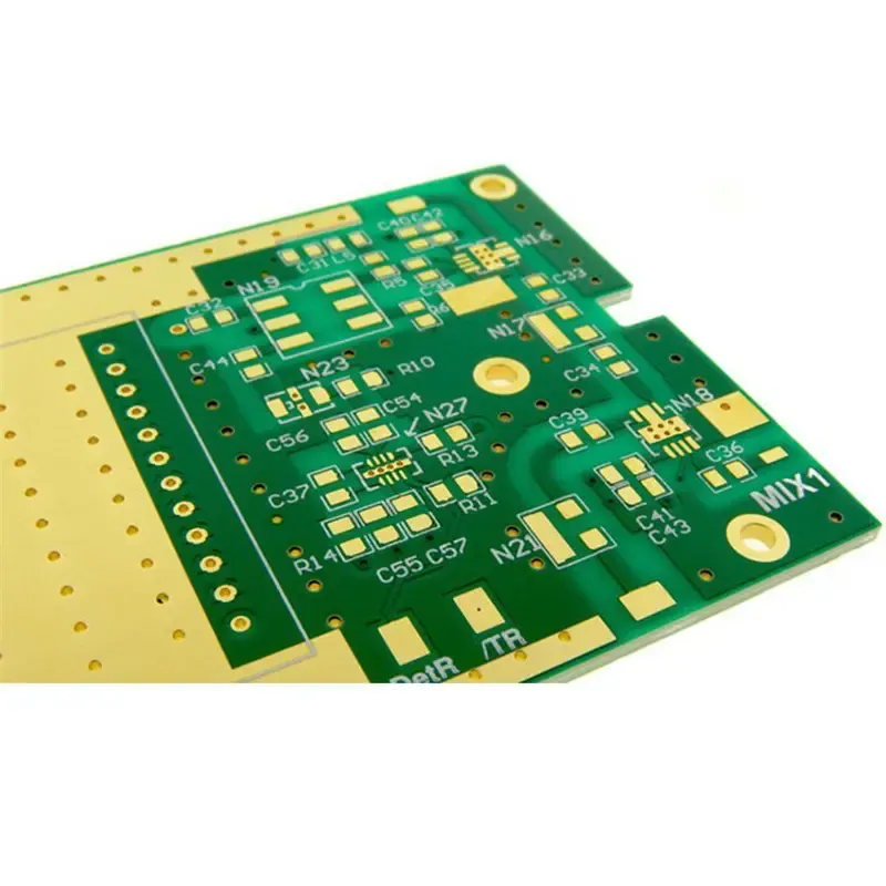
When reviewing options such as How Do I Select RF PCB Materials?, engineers must evaluate four core physical variables during stackup planning:
Dielectric Constant ($D_k$ / $\varepsilon_r$) Stability
Dielectric constant determines signal propagation velocity ($v_p = c / \sqrt{\varepsilon_r}$) and trace dimensions for a given target impedance. Lower $D_k$ values (typically 2.1 to 3.8) allow wider trace geometries, reducing fabrication tolerance sensitivity. However, for compact layouts, high-$D_k$ materials (6.0 to 10.2+) shrink wavelength dimensions, permitting smaller filter networks and patch antennas. Crucially, $D_k$ must remain stable across your operating temperature range (evaluated via Thermal Coefficient of Dielectric Constant, or $TC D_k$) and across your operating frequency spectrum.
Dissipation Factor (Loss Tangent, $\tan\delta$ / $D_f$)
Dissipation factor measures energy lost as heat within the dielectric dielectric matrix. Standard FR-4 exhibits a $D_f$ of ~0.020, which converts significant RF power into thermal loss above 1 GHz. Advanced RF laminates maintain $D_f$ values between 0.0009 and 0.0035, suppressing signal attenuation over long transmission lines. Evaluating $D_f$ is vital for high-power power amplifiers and sensitive low-noise receivers.
Copper Foil Surface Roughness
At high frequencies, the skin effect concentrates electrical current into a thin outer layer of the copper trace. The skin depth ($\delta$) decreases inversely with the square root of frequency:
$$\delta = \sqrt{\frac{\rho}{\pi f \mu}}$$
If the copper surface roughness ($R_z$) approaches or exceeds the skin depth, current travels along the micro-contours of the copper tooth profile, substantially increasing phase delay and conductor loss. Standard electrodeposited (ED) copper features roughness around 3 to 6 µm, whereas Very Low Profile (VLP) and Very-Very Low Profile (HVLP) copper foils keep profile heights below 1.2 µm, making them essential above 10 GHz.
Thermal and Mechanical Compatibility
RF power amplifiers generate localized heat that requires substrates with high thermal conductivity ($k \ge 0.5 - 1.0\text{ W/m}\cdot\text{K}$) compared to standard FR-4 ($0.25\text{ W/m}\cdot\text{K}$). Additionally, the Coefficient of Thermal Expansion (CTE) along the X, Y, and Z axes must match copper ($16-17\text{ ppm/}^\circ\text{C}$) to prevent barrel cracking in plated through-holes (PTH) and microvias during reflow soldering cycles.
> Manufacturing Rule of Thumb: Always request material datasheets that specify $D_k$ measured via the IPC-TM-650 2.5.5.5 clamped stripline test method at your specific operational frequency, rather than relying on single-point 1 MHz values.
Commonly Used RF PCB Materials and Their Trade-offs
No single laminate substrate satisfies every design parameter. Balancing performance against fabrication cost and mechanical stability leads engineers to four primary material families.
1. PTFE-Based Laminates (Polytetrafluoroethylene)
Pure PTFE delivers exceptional electrical performance, boasting a dielectric constant near 2.1 and dissipation factors down to 0.0009. However, pure PTFE suffers from high Z-axis thermal expansion and cold-flow deformation under mechanical pressure. To fix this, manufacturers reinforce PTFE with woven glass or ceramic filler materials:
- Woven Glass Reinforced PTFE: Increases dimensional stability and mechanical strength while maintaining $D_k$ between 2.17 and 2.50. However, the glass weave pattern can cause localized $D_k$ micro-variations (skew) beneath microstrip lines.
- Ceramic-Filled PTFE: Incorporates micro-ceramic particles to achieve $D_k$ values from 3.0 to 10.2 while lowering Z-axis CTE to match copper ($24-30\text{ ppm/}^\circ\text{C}$). This profile minimizes thermal stress on plated vias during PCBA reflow.
2. Hydrocarbon-Ceramic Laminates
Hydrocarbon-ceramic thermoset materials combine low electrical loss ($D_f \approx 0.002 - 0.004$) with physical stiffness similar to FR-4. These thermoset polymers do not require specialized pre-treatment before electroless copper deposition, making them easier to process in high-volume PCBA manufacturing facilities. They operate effectively up to 20 GHz and pair well with conventional SMT line operations.
3. Thermoset Modified PPE/PPO Resins
Polyphenylene Ether (PPE) and Polyphenylene Oxide (PPO) resins bridge the performance gap between enhanced FR-4 and pure hydrocarbon systems. Offering $D_f$ values around 0.003 to 0.006 up to 10 GHz, these thermoset systems provide excellent thermal resistance ($T_g > 180^\circ\text{C}$), high glass transition limits, and good adhesion to smooth copper foils.
4. Enhanced High-$T_g$ FR-4
While traditional FR-4 is unsuitable for microwave designs, enhanced high-$T_g$ FR-4 laminates ($T_g \ge 170^\circ\text{C}$) feature tighter resin formulation controls and reduced loss tangents ($D_f \approx 0.010 - 0.012$). They are cost-effective choices for control circuitry, digital interfaces, and sub-1 GHz RF links where trace lengths remain short.
For flexible and rigid-flex designs operating at high frequencies, review the Flex PCB Manufacturing Process: Materials Selection, Etching, & Lamination for polyimide substrate parameters.
Stackup Architecture and Hybrid PCB Designs
Building a pure RF stackup using high-frequency laminates for all dielectric layers can dramatically increase raw board costs. To optimize total unit economics, engineers frequently implement hybrid stackup configurations.
Hybrid Stackup Engineering Guidelines
A hybrid stackup pairs high-frequency laminates on outer layers (where RF microstrip or coplanar waveguides reside) with standard FR-4 cores and prepregs on inner layers for power distribution and low-speed control routing. When designing hybrid stackups, observe these core rules:
1. Thermal Expansion Coefficient Alignment: Ensure the $Z$-axis CTE of the FR-4 prepreg closely matches the RF core to prevent delamination during reflow temperatures ($260^\circ\text{C}$). Standardize cure temperature profiles across chosen prepreg systems. 2. Symmetrical Material Distribution: Balance layer thicknesses and material types around the central neutral axis to suppress bow and twist after lamination. Unbalanced hybrid stackups frequently fail automated optical inspection or SMT placement tolerances. 3. Resin Flow and Cavity Filling: Choose prepreg glass styles (e.g., 106, 1080, 2116) with adequate resin content ($%\text{ Resin}$) to fill copper patterns on adjacent RF reference planes without resin starvation or voiding.
Addressing stackup imbalances early prevents costly engineering changes. Learn more about preventing layout defects in Common DFM Issues and How to Avoid Them in PCB Design.
Manufacturing Challenges, DFM Rules, and Reliability
Fabricating RF printed circuit boards introduces physical processing challenges that differ significantly from standard digital board production. Selecting an RF material requires evaluating how the material behaves during drilling, etching, plating, and testing.
Drilling and Hole Wall Preparation
Soft PTFE substrates tend to smear under mechanical drill bit action, causing thermal plastic residue to coat internal copper land rings. Removing drill smear from PTFE requires specialized sodium naphthenate treatment or plasma etching (plasma desmear) prior to electroless copper plating. Standard permanganate chemical desmear processes used for FR-4 are ineffective on fluoropolymers. Failing to plan for plasma processing results in poor hole-wall copper adhesion and inter-layer interconnect failures.
Etch Tolerances and Impedance Precision
Controlled-impedance RF traces require tight line-width tolerances (often $\pm 0.5\text{ mil}$ or $\pm 10\mu\text{m}$). As etching solution removes copper, it creates an etch factor (trapezoidal trace cross-section). Fabricators must compensate Gerber artwork trace widths based on copper foil thickness (e.g., 0.5 oz vs 1 oz copper).
For high-power RF circuits incorporating heavy copper layers, refer to Common Failures in Heavy Copper PCB and How to Avoid Them in the Design Stage to evaluate thermal stress tradeoffs.
Surface Finish Selection
The surface finish applied to exposed RF pads directly affects solderability and insertion loss. Nickel-based finishes like ENIG (Electroless Nickel Immersion Gold) introduce a ferromagnetically lossy nickel layer between the copper trace and gold coating. At frequencies above 5 GHz, this nickel layer increases signal attenuation. Preferred finishes for high-frequency circuits include:
- Silver (Immersion Silver / ImAg): Provides smooth planar surfaces with negligible conductor loss.
- ENEPIG: Excellent for wire bonding, though nickel attenuation must still be modeled above 10 GHz.
- Bare Copper with OSP (Organic Solderability Preservative): Preserves signal integrity at minimal loss, though it offers limited shelf-life and handling cycles.
Electrical Testing and Verification
Verifying trace geometry and impedance accuracy across production lots requires systematic testing. Flying probe systems and time-domain reflectometry (TDR) verify interconnect continuity and impedance performance without requiring custom bed-of-nails fixtures. Read the detailed breakdown on Demystifying Flying Probe PCB Testing: The What, Why, and How for fixtureless test setups.
RF PCB Material Selection Matrix
The following table compares primary RF material families across key IPC-4101 / IPC-6012 performance parameters:
| Material Family | Dielectric Constant ($D_k$ @ 10 GHz) | Dissipation Factor ($D_f$ @ 10 GHz) | Thermal Conductivity (W/m·K) | Relative Material Cost | Standard Fabrication Processing | Primary Application Spectrum |
|---|---|---|---|---|---|---|
| High-$T_g$ FR-4 | 3.8 – 4.3 | 0.015 – 0.020 | 0.25 – 0.35 | Low (1x) | Standard FR-4 Line | Sub-1 GHz, Control, Power |
| Hydrocarbon-Ceramic | 3.38 – 3.55 | 0.0021 – 0.0037 | 0.60 – 0.80 | Moderate (3x – 4x) | Direct FR-4 Compatible | 1 GHz – 20 GHz, Sub-6 GHz 5G |
| Thermoset PPE/PPO | 3.0 – 3.5 | 0.0030 – 0.0050 | 0.35 – 0.50 | Moderate (2.5x – 3.5x) | Direct FR-4 Compatible | 1 GHz – 15 GHz, Automotive Radar |
| Woven Glass PTFE | 2.17 – 2.50 | 0.0009 – 0.0019 | 0.20 – 0.45 | High (6x – 8x) | Requires Plasma Desmear | 20 GHz – 80 GHz, Satellite Comms |
| Ceramic-Filled PTFE | 3.0 – 10.2 | 0.0015 – 0.0025 | 0.50 – 1.30 | Very High (8x – 12x) | Requires Plasma Desmear | Defense, Space, High-Density Radar |
Critical DFM Checklist for RF Material Selection
Before submitting your RF PCB stackup and Gerber fabrication files for manufacturing review, verify these critical review items with your EMS partner Omini:
- [ ] Specify Material Grade and Manufacturer: Name exact series (e.g., Rogers RO4003C, Isola IS680, Taconic TLX) rather than generic labels like "PTFE" or "RF substrate."
- [ ] Verify $D_k$ Value at Target Frequency: Ensure stackup impedance calculations use $D_k$ values evaluated at your operating frequency rather than default 1 MHz reference values.
- [ ] Call Out Copper Foil Profile: State whether Standard ED, VLP, or HVLP copper foil is required for signal-critical layers.
- [ ] Include IPC Specification Context: Reference IPC-4101 laminate sheets and IPC-6012 Class 2 or Class 3 inspection criteria on engineering drawings.
- [ ] Confirm Hybrid Prepreg Compatibility: Check that prepreg glass styles provide sufficient resin fill percentage over etched copper planes.
- [ ] Select RF-Friendly Surface Finish: Avoid standard ENIG on signals above 5 GHz if loss budgets are tight; opt for Immersion Silver or OSP where applicable.
- [ ] Validate Drill-to-Copper and Via Aspect Ratios: Maintain mechanical drill aspect ratios below 10:1 for reliable plated through-hole copper coverage in thick hybrid stackups.
When preparing complex high-frequency projects for Omini review, connect material callouts, stackup symmetry, and DFM tolerances to actual factory-floor limits before release. Early coordination reduces avoidable redesign cycles.