
Direct Answer
The most common DFM issues in PCB design stem from a disconnect between what EDA tools allow and what fabrication and assembly lines can repeatably produce. Thin traces, tight annular rings, non-standard drill sizes, and component footprints that ignore solder mask tolerances all pass electrical rule checks—then fail in production, triggering respins, expedite fees, and missed market windows. The fix is straightforward: treat your manufacturer as a design partner, not a downstream vendor, and validate every critical dimension against their process capability matrix before releasing Gerbers.
Why DFM Failures Slip Through Electrical Validation
Most design teams validate layouts against electrical constraints—impedance, crosstalk, power integrity—while treating mechanical and process rules as secondary. The result is a board that simulates perfectly but cannot be manufactured at yield. A trace width specified at 3 mil may be electrically sound, yet unsupported by standard etching processes without premium pricing. A via placed too close to a pad may pass DRC, but create solder wicking during reflow that starves the joint.
The root cause is often toolchain fragmentation. PCB designers work in layout environments that know little about the specific photoplotter, drill station, or lamination press that will produce the board. Without explicit DFM feedback loops, the first time these issues surface is often in a fabricator's engineering query—after the design is supposedly complete.
Stackup and Impedance Mismatches That Kill Schedules
Impedance-controlled designs demand tight cooperation between designer and fabricator. A common mistake is specifying dielectric constants and prepreg thicknesses from generic datasheets, then expecting the fabricator to hit target impedance without deviation. In practice, every shop maintains a calibrated set of standard stackups based on their actual laminate inventory, press cycle, and controlled impedance test coupon history.
Deviating from these standards forces custom builds: non-standard core thicknesses, exotic low-Dk materials, or additional lamination cycles. Each adds cost and lead time. For high-speed designs, the better path is to share your target impedance and insertion loss budget early, then let your fabricator propose a validated stackup that meets electrical requirements within their standard process window.
For a deeper look at how layer ordering and material selection affect signal quality, see our guide on PCB Stack-Up and Signal Integrity for High-Speed Boards.
Annular Rings, Copper Slivers, and Acid Traps
Annular ring violations are among the most frequent fabrication rejects. The annular ring is the copper pad area surrounding a drilled hole. When design rules push this margin below the fabricator's capability, the drill may break out into the pad edge, compromising via reliability or component lead solderability. The fix is not merely to meet a minimum number in a datasheet, but to understand your manufacturer's drill registration accuracy and their preferred annular ring targets for different via types.
Copper slivers—thin, isolated copper remnants between closely spaced features—create similar risks. During etching, slivers can detach and redeposit elsewhere on the panel, causing shorts. Acid traps, formed by acute-angle traces entering pads, concentrate etchant and create over-etched regions that weaken traces or create opens. Both issues are preventable with simple layout hygiene: maintain adequate spacing, avoid acute angles on copper pours, and run a dedicated DFM check for sliver and trap conditions.
Component Spacing and SMT Assembly Reality
DFM for assembly means designing for the pick-and-place nozzle, the reflow oven profile, and the inspection camera—not just the schematic symbol. Components placed too close together may pass DRC yet fail in production due to nozzle interference, uneven heating, or blocked optical inspection paths. Fine-pitch QFNs and passives near large thermal mass components create particular risk: the small part reflows differently, leading to tombstoning or insufficient solder joints.
At Omini, our EMS teams regularly see designs where test points are buried under connectors or positioned where probes cannot reach. Adding testability after layout completion means rework, not design. The better approach is to reserve accessible test point locations during placement, ensure adequate keepout zones around high-pin-count devices, and verify that fiducial placement supports the vision systems on your assembler's SMT lines.
Surface Finish Selection as a DFM Decision
Surface finish is too often treated as a late procurement decision rather than a design parameter. Yet finish choice directly affects solder joint reliability, shelf life, and assembly process window. ENIG offers flatness and long shelf life but requires careful control to avoid black pad defects. HASL is economical but introduces topography challenges for fine-pitch components. OSP provides excellent solderability within its limited storage window but demands stricter handling protocols.
The DFM implication is clear: your finish must match your component mix, your storage and shipping model, and your assembly thermal profile. Selecting HASL for a 0.4 mm pitch BGA because it is cheaper is a false economy if it drives placement defects or requires additional rework. For a detailed comparison of tradeoffs, read ENIG vs OSP vs HASL for PCB Manufacturing.
Rigid-Flex and the Unique DFM Considerations
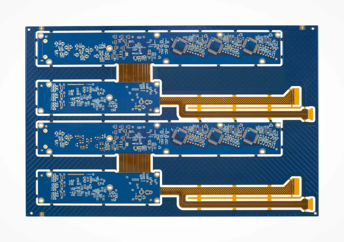
Rigid-flex designs introduce mechanical and material constraints that do not exist in rigid-only boards. Bend radius, flex layer count, coverlay overlap, and adhesive flow control all require early manufacturer involvement. A common error is designing bend regions with copper features that experience fatigue cracking after a few flex cycles, or specifying rigid-flex constructions that exceed standard material availability.
The transition zone between rigid and flex sections demands particular attention. Plated through-holes in this region experience stress concentration; vias should be kept clear of the bend line by distances specified by your fabricator's capability. For practical guidance on these constraints, review Rigid-Flex PCB DFM Tips Before PCB Manufacturing.
Gerber and Documentation Gaps That Delay First Article
Even electrically perfect designs stall when documentation is incomplete or ambiguous. Missing layer assignments, unclear board outline definitions, and unspecified copper weights are frequent culprits. Gerber files that omit solder mask and paste mask layers, or that use non-standard aperture lists, force manual interpretation by CAM engineers—introducing delay and the potential for misinterpretation.
A robust documentation package includes: Gerber RS-274X for all copper, mask, and silk layers; an IPC-356 netlist for electrical test generation; a clearly structured BOM with manufacturer part numbers; and a fabrication drawing specifying stackup, controlled impedance requirements, surface finish, and any special instructions. Investing an hour in documentation completeness can save days in engineering query cycles.
Cost Implications of Ignoring DFM
DFM oversights do not always cause outright failure. More commonly, they inflate cost through subtle channels: premium pricing for non-standard features, yield loss that drives unit economics upward, or expedited freight to recover schedule slippage. A design that requires laser drilling for aspect ratio control, for example, may multiply drilling costs compared to a mechanically drilled alternative. Tight trace-and-space rules that push fabrication to the process limit often trigger lot charges or minimum order premiums.
Understanding these cost drivers requires viewing DFM not as a constraint but as a negotiation between functionality and process capability. The goal is not the cheapest board, but the most reliable board at the target cost. For perspective on how poor early decisions compound budget problems, see Cheap PCB Manufacturing: Common Mistakes That Kill Your Budget.
Building DFM Into Your Design Workflow
Effective DFM integration means shifting checks left in the design cycle. Rather than a single pre-release review, implement staged DFM gates: stackup validation after layer assignment, component spacing review during placement, and a full Gerber DFM run before final release. Many modern EDA tools offer DFM rule sets, but these are generic. Calibrating them against your specific manufacturer's capability matrix yields far more actionable results.
Equally important is maintaining a feedback loop. When boards return from fabrication or assembly with defects, trace whether the issue was detectable at design stage. Over time, this builds an organization-specific DFM knowledge base that improves first-pass yield and reduces reliance on external review.
Inspection and Testability from the Layout Stage
DFM extends through to how a board will be verified. Automated Optical Inspection (AOI) and X-ray inspection are standard in modern PCB assembly, but their effectiveness depends on layout decisions made long before the first component is placed. Components oriented at odd angles, pads obscured by taller neighboring parts, or insufficient solder joint visibility all limit inspection coverage.
For complex assemblies—especially those with hidden solder joints under QFNs or BGAs—X-ray inspection is essential. Yet even X-ray has blind spots if via-in-pad designs are not optimized or if component density creates overlapping images. Designing with inspection access in mind means preserving line-of-sight to critical joints, orienting components consistently for AOI algorithms, and including adequate test points for in-circuit or flying probe test. Learn more about how these methods work together in AOI and X-Ray Inspection in PCB Assembly.
Final Field Note
DFM is not a checklist to complete before sending files to your fabricator. It is a continuous conversation between design intent and manufacturing reality, conducted in the language of process limits, material properties, and economic tradeoffs. The teams that treat this conversation as integral to design—rather than an afterthought—are the ones that ship on time, hit cost targets, and build products that survive in the field. Start that conversation early, keep it specific, and let your manufacturer's capability data guide decisions that your simulation tools alone cannot make.