
Direct Answer
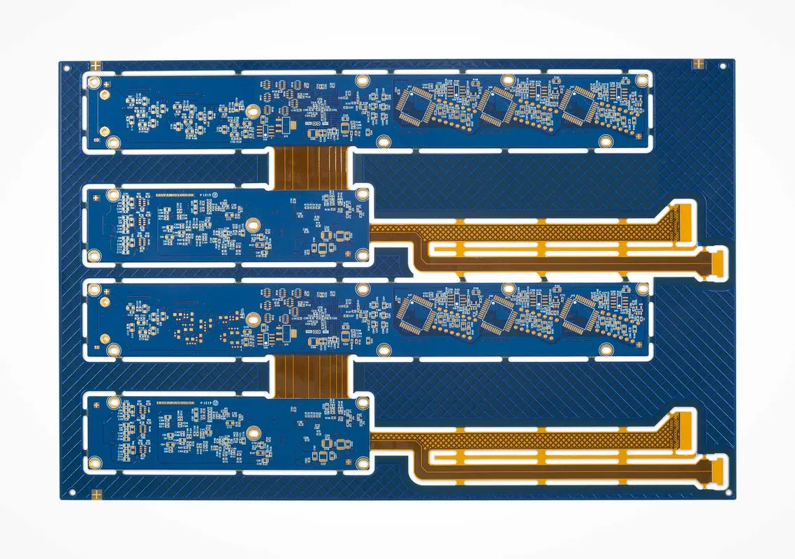
Rigid flex PCBs combine rigid and flexible substrate layers into a single interconnect system, replacing multiple rigid boards, cables, and connectors with one integrated structure. Engineers choose them when space is constrained, vibration resistance matters, or assembly complexity drives cost. The technology reduces failure points and improves signal integrity, but it demands careful stackup planning and DFM review before fabrication. Understanding bend radius, material selection, and layer transitions is essential for a successful build.
---
Why Rigid Flex PCBs Replace Cable Assemblies and Multiple Boards
A rigid flex PCB is not simply a flexible circuit with stiffeners attached. It is a single laminated structure where rigid sections provide mechanical support for component mounting and flexible sections route signals between those rigid zones. The flex layers are typically polyimide-based, while the rigid sections use standard FR-4 or other rigid laminates bonded to the flex core.
The primary engineering driver is interconnect consolidation. A product that would traditionally use two or three rigid PCBs joined by ribbon cables, wire harnesses, or board-to-board connectors can be redesigned as one rigid flex assembly. This eliminates:
- Connector solder joints, which are common failure points under vibration
- Cable routing errors during manual assembly
- Inventory complexity from multiple part numbers
- Space consumed by connectors and cable bend radius
From a manufacturing standpoint, the assembly process also simplifies. Instead of populating separate boards and then performing a secondary cable attach operation, the entire interconnect is already part of the board. This reduces labor hours per unit and removes a significant source of human error. For high-reliability applications such as medical implants, aerospace avionics, or military radios, the reliability gain from eliminating dozens of solder joints often justifies the higher base cost of the rigid flex substrate itself.
The trade-off is upfront engineering effort. A rigid flex design requires the designer to think in three dimensions from the start. The flex regions must be planned for their actual bending motion, not treated as an afterthought. The stackup must be defined before layout, not adjusted after routing is complete. This is why the design review phase is more critical for rigid flex than for conventional rigid PCBs.
---
Rigid Flex Stackup Construction and Material Selection
Layer Structure and Transitions
A typical rigid flex stackup alternates rigid layers and flex layers. The flex core is usually one or two copper layers on polyimide, with adhesive bonding the layers together. Rigid layers are laminated on top of the flex core only in the areas where components will be mounted. The transition zone—where the rigid laminate ends and the flex area begins—is the most sensitive region in the entire board.
The transition requires a gradual step-down rather than an abrupt cut. If the rigid laminate terminates too sharply, stress concentrates at that point during bending, leading to delamination or copper cracking. Most manufacturers recommend a teardrop or fillet shape at the rigid-to-flex boundary, and the flex layer should extend slightly beyond the rigid layer edge to distribute strain.
Copper weight selection also differs between rigid and flex sections. Standard rigid boards often use 1 oz or 2 oz copper. Flex circuits, especially dynamic ones, typically use 0.5 oz (18 µm) or even 0.25 oz (9 µm) copper because thinner copper withstands repeated bending better. If the design requires higher current in a flex region, consider widening the trace instead of increasing copper weight. A wider trace distributes stress more evenly than a thicker trace of the same width.
Material Choices and Their Impact
Polyimide is the dominant flex dielectric material because of its thermal stability, chemical resistance, and mechanical durability. The base material is typically a polyimide film such as Kapton, laminated with acrylic or epoxy adhesive. Adhesive-free materials exist and offer better dimensional stability and thermal performance, but they cost more and may have longer lead times.
For the rigid sections, standard FR-4 is usually sufficient. However, the laminate must be compatible with the flex material in terms of coefficient of thermal expansion (CTE) and processing temperature. If the board will experience wide temperature swings, consider a lower-CTE rigid laminate to reduce stress at the flex-rigid interface.
For a deeper look at material options and their trade-offs, see our article on Flex PCB Material: Construction, Classification, and Advantages. The material selection process for rigid flex follows the same logic, with the added constraint that rigid and flex materials must be compatible in lamination.
Coverlay vs. Solder Mask
Flex regions use coverlay (a polyimide film with adhesive) rather than solder mask. Coverlay provides better flexibility and protects the copper from handling damage. Solder mask on flex areas tends to crack during bending. The coverlay must be registered accurately to the copper pattern, and openings must be provided where components or vias need access.
A common mistake is designing coverlay openings too small. The adhesive squeezes out during lamination, reducing the effective opening size. If a pad is partially covered by adhesive, solderability suffers. Always add 0.1 mm to 0.15 mm of clearance around the pad on the coverlay opening, and confirm the manufacturer's registration tolerance before finalizing the artwork.
---
Dynamic vs. Static Flexing: What to Specify in Your RFQ
The single most important question to answer before designing a rigid flex PCB is whether the flex regions will bend dynamically (during product use) or statically (bent once during installation and then held in place). This distinction drives material selection, copper weight, bend radius, and even the number of flex layers allowed.
Dynamic flexing requires:
- Thinner copper (0.5 oz or less)
- Larger minimum bend radius (typically 10x the flex thickness or more)
- Adhesive-free or low-adhesive materials
- Fewer flex layers (1-2 preferred)
- Cross-hatched or hatched copper planes instead of solid pours
Static flexing allows:
- Standard 1 oz copper in flex areas
- Smaller bend radius (5x to 6x the flex thickness)
- More flex layers (up to 4-6 in some cases)
- Solid copper pours if needed for shielding or current
If you do not specify dynamic vs. static in the RFQ, the manufacturer will assume static flexing by default. This can lead to field failures if the product actually flexes during use. Conversely, specifying dynamic when the application is static adds unnecessary cost and may restrict design options.
The operating environment matters too. A flex region that bends once at room temperature during assembly is very different from one that flexes thousands of times at -40°C. If temperature extremes are involved, the bend radius must increase and the material selection must account for the change in mechanical properties at temperature.
For a complete overview of how flex circuits are manufactured and where the process constraints come from, review our Flex PCB Manufacturing Process: An Overview for Beginners. The rigid flex process builds on these same steps, adding the rigid lamination and transition zone management.
---
Design Rules and DFM Review for Rigid Flex
Minimum Bend Radius
The minimum bend radius is the most frequently violated design rule in rigid flex. It depends on the flex layer thickness, copper weight, and whether the application is dynamic or static. A general rule of thumb:
| Application | Minimum Bend Radius (relative to flex thickness) |
|---|---|
| Static, one-time bend | 5x to 6x |
| Dynamic, repeated bending | 10x or greater |
| Dynamic with thick copper (>1 oz) | 15x or greater |
These are starting points, not absolute values. The actual radius depends on the specific stackup and material. Always confirm with the manufacturer before finalizing the design. If space constraints force a smaller radius, consider reducing the flex layer thickness or switching to a thinner copper weight.
Via and Pad Placement
Vias and through-hole pads should never be placed in the bend region. The copper plating inside a via is rigid and will crack under repeated bending. If a via must be near a bend area, keep it at least 2-3 mm away from the start of the bend zone. The same applies to large surface-mount components—they create local stiffness that concentrates stress at their edges.
Stiffeners and Their Role
Stiffeners are additional polyimide or FR-4 layers added to flex regions to provide mechanical support for component mounting or connector attachment. They are not the same as rigid sections—they do not contain copper layers and are bonded only to the flex area.
Stiffener placement must be specified in the fabrication drawing. Common mistakes include:
- Placing a stiffener too close to the bend line, which creates a stress concentration at the stiffener edge
- Using a stiffener that is too thick, which increases the overall flex region thickness and reduces flexibility
- Forgetting to account for stiffener thickness in the overall board thickness calculation, which affects component standoff and enclosure fit
DFM Review Checklist
Before sending files to fabrication, perform a structured DFM review. The checklist should include:
- Bend radius vs. flex thickness ratio, confirmed with the manufacturer
- Via and pad clearance from the bend zone (minimum 2 mm)
- Coverlay opening sizes with adequate clearance for adhesive squeeze-out
- Stiffener placement and thickness relative to the bend line
- Layer transition geometry at the rigid-flex boundary
- Copper weight in flex areas vs. current-carrying requirements
- Flex layer count vs. dynamic flexing requirements
- Panel utilization—rigid flex boards often have lower panel utilization than rigid boards, which affects cost
For a broader understanding of how flex manufacturing constraints affect the process, see Flex PCB Manufacturing Process: Materials Selection, Etching, & Lamination. The etching and lamination steps are where many rigid flex defects originate.
---
Assembly, Inspection, and Reliability Considerations
SMT Assembly Handling
Rigid flex boards require different handling than rigid boards during SMT assembly. The flex regions can bend or twist during pick-and-place, causing misalignment or component tombstoning. Use pallets or fixtures that support the entire board, including the flex areas, during solder paste printing and reflow.
The reflow profile itself is generally the same as for rigid boards, but the thermal mass of the board varies significantly between rigid and flex sections. This can cause temperature gradients across the board during reflow. If the flex section is thin and the rigid section is thick, the flex area may reach peak temperature faster, potentially causing warpage. Work with your assembly partner to verify the profile on the actual board, not just on a test coupon.
Inspection Challenges
Visual inspection of rigid flex boards is more complex than rigid boards. The flex layer alignment and coverlay registration must be checked, and the transition zones require close examination for delamination or adhesive voids. Automated optical inspection (AOI) systems may need custom fixtures to hold the board flat without stressing the flex areas.
Electrical testing also requires care. A flying probe or fixture that applies pressure to the flex region can damage the board. Use test fixtures that support the flex areas from underneath and avoid applying force directly to the bend zones.
Reliability Qualification
For qualification, IPC-6012 covers rigid PCB performance and IPC-6013 covers flexible and rigid flex PCB performance. These standards define the acceptance criteria for things like conductor spacing, plating quality, and flexural endurance. However, the standards do not define every parameter—your manufacturer may have additional internal criteria that are stricter.
If your application involves dynamic flexing, request flexural endurance testing. This test bends the flex region repeatedly to a specified radius and verifies that the conductors do not crack. The number of cycles depends on the application—a wearable device might need 100,000 cycles, while a medical device might need only 10,000. Specify the expected cycle count and bend radius in the RFQ so the manufacturer can select appropriate materials and test methods.
> Practical note: If your product flexes dynamically, do not rely solely on IPC-6013 acceptance criteria. That standard covers the manufacturing quality, but it does not guarantee that your specific bend radius and cycle count will survive in the field. Simulate or prototype the actual motion early in the design cycle.
---
Common Mistakes and How to Avoid Them
Mistake 1: Ignoring the Bend Radius
The most common error is designing a bend that is too tight for the stackup. The designer sees the flex area as "thin" and assumes it can bend sharply. In reality, the minimum bend radius is a function of the total flex thickness, including coverlay and adhesive layers. A 0.2 mm flex core with 0.05 mm coverlay on each side has a total thickness of 0.3 mm, which at 10x gives a 3 mm minimum bend radius. That is not a sharp fold.
Mistake 2: Placing Vias in the Bend Zone
Vias create rigid columns through the flex material. When the flex region bends, the via barrel cracks. This is a field failure that is difficult to detect during inspection because the crack may be intermittent. Keep vias completely out of the bend area, and if a via must be near the bend, use a teardrop connection to the trace.
Mistake 3: Not Specifying Dynamic vs. Static
As discussed earlier, this single omission can lead to a board that works in the lab but fails in the field. If you are unsure whether the application is dynamic or static, assume dynamic and design for it. The cost difference is usually modest compared to the cost of a field failure.
Mistake 4: Poor Coverlay Registration
Coverlay openings that are too small or misregistered relative to the pads cause solderability issues. The adhesive squeeze-out reduces the effective opening. Always account for the manufacturer's registration tolerance and add clearance to the coverlay artwork.
Mistake 5: Forgetting Stiffener Effects
Stiffeners add thickness and rigidity to flex areas, but they also create stress concentrations at their edges. If a stiffener ends too close to a bend line, the flex material will crease at the stiffener edge during bending. Place stiffeners at least 2-3 mm away from the bend zone.
---
What to Include in Your RFQ
A complete RFQ for a rigid flex PCB should include more than just Gerber files. The manufacturer needs to understand the application and the mechanical requirements to make correct decisions about materials and processing.
Include the following in your RFQ:
- Complete layer stackup with material types, thicknesses, and copper weights for each layer
- Flex layer count and which layers are flex vs. rigid
- Bend radius and whether flexing is dynamic or static
- Expected number of flex cycles if dynamic
- Operating temperature range
- Stiffener locations, materials, and thicknesses
- Coverlay openings and any special registration requirements
- Surface finish (ENIG, immersion silver, etc.) for both rigid and flex areas
- Any testing requirements (flexural endurance, impedance control, etc.)
- Reference to IPC-6013 for flex performance and IPC-6012 for rigid sections
The more context you provide, the more accurate the quote and the fewer surprises during fabrication. If you are unsure about any parameter, ask the manufacturer for guidance before finalizing the design. A quick conversation early in the design phase is far cheaper than a redesign after fabrication.
For a comparison with simpler board types, see our article on Double Sided PCB: Advantages, Applications, and Manufacturing Process. Double-sided rigid boards are often the starting point before a design evolves into rigid flex.
---
Practical Example: A Wearable Medical Device
Consider a wearable heart monitor that must fit in a 30 mm × 40 mm enclosure. The design requires a main processor board, a sensor board, and a flexible connection between them that bends 90 degrees during assembly and then stays static.
A rigid flex design would use:
- Rigid section 1: 4-layer FR-4, 1 oz copper, 0.8 mm thick, housing the processor and power management
- Rigid section 2: 2-layer FR-4, 1 oz copper, 0.6 mm thick, housing the sensor and analog front end
- Flex section: 2-layer polyimide, 0.5 oz copper, 0.2 mm total thickness, connecting the two rigid sections
- Bend radius: 2 mm (static, one-time bend during assembly)
- Stiffener: 0.3 mm polyimide stiffener under the sensor pads on the flex section
The stackup drawing must show the transition zones where the FR-4 layers terminate and the flex layers continue. The coverlay openings must be sized for the sensor pads, and the stiffener must end at least 2 mm from the bend line.
During assembly, the board is populated flat, then bent into its final shape during enclosure assembly. The static bend means the flex region does not need dynamic flex testing, but it should still be inspected for copper cracking after the bend is formed.
This design replaces what would otherwise be two rigid boards, a 12-pin connector, and a short cable assembly. The rigid flex version eliminates the connector and cable, reduces assembly time by roughly 15 minutes per unit, and improves reliability by removing 24 solder joints from the signal path.
---
When to Involve the Manufacturer
Involve the manufacturer early—ideally during the stackup definition phase, not after the layout is complete. The stackup determines the bend radius, the material availability, and the panel utilization. If you design the stackup without manufacturer input, you risk specifying materials that are not stocked or a flex thickness that is not manufacturable.
Omini's engineering team can review your stackup and bend requirements before you commit to the layout. This review typically takes a few hours and can save weeks of redesign time. The earlier the review, the more flexibility you have to adjust the design without impacting the schedule.
Also involve the manufacturer if you are uncertain about the dynamic vs. static classification. An experienced manufacturing engineer can help you assess the actual motion in your product and recommend appropriate design rules. This is especially important for products with complex kinematics, such as foldable devices or articulated robotic arms.
For a foundational understanding of flex circuit technology, start with our Introduction to Flex PCBs: Basics and Benefits for Reliable PCBA. That article covers the core concepts that apply to rigid flex as well.
---
FAQ
Q: Why choose a rigid flex PCB instead of separate rigid boards and cables?
A: Rigid flex PCBs integrate rigid sections for component mounting and flexible sections for routing between them. This reduces connectors, solder joints, and wiring harnesses, which improves reliability and saves space. It also simplifies assembly because the interconnect is part of the board, not a separate cable.
Q: Where do engineers commonly make mistakes when designing rigid flex PCBs?
A: Common mistakes include ignoring the minimum bend radius, placing vias or pads too close to the bend area, and not specifying dynamic vs. static flexing. Engineers also forget to account for coverlay openings or adhesive squeeze-out, which can affect component placement and solderability.
Q: How can I verify a rigid flex PCB design before sending it to fabrication?
A: Perform a DFM review with your manufacturer, focusing on layer stackup, bend radius, and material selection. Use IPC-2221 and IPC-2223 as design guidelines, and provide a detailed stackup drawing with copper weights, dielectric types, and flex layer materials. Also, simulate or prototype the flexing motion if the application is dynamic.
Q: What information should I include in an RFQ for a rigid flex PCB?
A: Include the complete layer stackup, material types (e.g., polyimide, adhesive), copper weights, bend radius and whether flexing is dynamic or static, number of flex layers, and any stiffener requirements. Also specify the operating temperature range, flexing cycles expected, and any testing requirements. Clear documentation helps the manufacturer quote accurately and avoid surprises.
Q: What are the typical applications for rigid flex PCBs?
A: Rigid flex PCBs are used in medical devices, aerospace electronics, military equipment, automotive systems, and consumer electronics where space is limited and reliability is critical. They are also common in wearable devices and any product with moving parts that require a flexible connection.
Q: How does rigid flex PCB construction affect assembly and inspection?
A: Rigid flex boards require careful handling during SMT assembly because the flex areas can bend or twist. Use pallets or fixtures to support the board during reflow. Inspection may need to account for flex layer alignment and coverlay registration, and electrical testing may require special fixtures to avoid stressing the flex regions.
> Engineering handoff note: Isola PCB Material: A Basic Introduction for Design and Manufacturing Decisions before the release package is frozen.