
Direct Answer
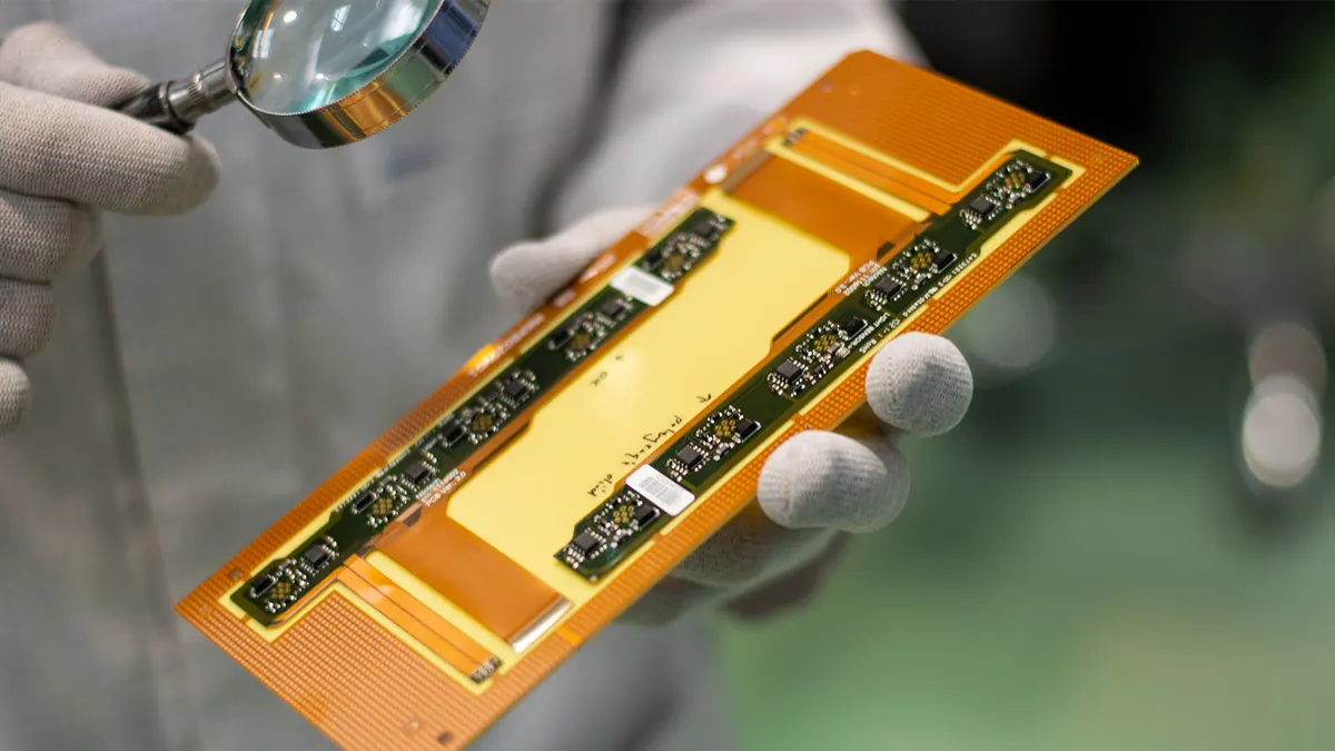
Flex PCBs are printed circuit boards built on flexible dielectric films, typically polyimide, that can bend, fold, and flex to fit into three-dimensional spaces where rigid boards cannot. They solve real packaging and reliability problems by reducing connectors, eliminating solder joints, and surviving repeated motion, but only when the stackup, copper type, and bend radius are matched to the actual application. A flex PCB is not simply a thin rigid board; it is a distinct engineering discipline.
What Makes a Flex PCB Different from a Rigid Board
The fundamental difference between a flex PCB and a rigid PCB is the base material system. Rigid boards use FR-4, a glass-reinforced epoxy laminate that is stiff and brittle. Flex boards use a thin, flexible dielectric film—most commonly polyimide (PI)—that can be bent repeatedly without cracking. The copper used in flex circuits is also different: it is typically rolled-annealed (RA) copper rather than electrodeposited (ED) copper. RA copper has a more ductile grain structure, which allows it to withstand repeated bending without fracturing.
The stackup of a flex PCB is also thinner and more carefully controlled. A typical single-sided flex stackup might be:
| Layer | Material | Typical Thickness |
|---|---|---|
| Coverlay | Polyimide + adhesive | 12.5–25 µm |
| Copper | RA or ED copper | 17.5–70 µm (0.5–2 oz) |
| Base film | Polyimide | 12.5–50 µm |
| Coverlay | Polyimide + adhesive | 12.5–25 µm |
The adhesive system matters as much as the film. Acrylic adhesives are common and inexpensive, but they have higher moisture absorption and lower thermal stability than no-flow or all-polyimide systems. For dynamic flex applications—where the circuit bends during operation—the adhesive must not creep or delaminate. For high-temperature or high-reliability applications, an all-polyimide construction with no adhesive is often specified, though it costs more.
The manufacturing process for flex boards also differs. Flex circuits are often processed in panels with stiffeners added later, and the etching and lamination steps require careful tension control to prevent dimensional distortion. If you are new to the process side, the Flex PCB Manufacturing Process: An Overview for Beginners explains how the material set drives each step from imaging to final cut.
Static vs. Dynamic Flex: The Design Decision That Drives Everything
The single most important question in flex PCB design is whether the application is static or dynamic. A static flex circuit is bent once during installation and then remains in that shape for the life of the product. A dynamic flex circuit is bent, flexed, or twisted repeatedly during operation—for example, in a printer carriage, a folding phone hinge, or a robotic joint.
This distinction changes the material selection, copper weight, and minimum bend radius. For static applications, ED copper is often acceptable because the circuit is not subjected to repeated stress. For dynamic applications, RA copper is strongly recommended because its grain structure is elongated and aligned, allowing it to withstand millions of flex cycles without cracking. The bend radius also changes: a dynamic flex circuit needs a larger bend radius relative to its thickness to keep strain within the copper's elastic limit.
As a rule of thumb, the minimum bend radius for a dynamic flex should be at least 10 times the total thickness of the flex stackup. For static flex, the minimum bend radius can be as low as 3 to 6 times the thickness, depending on the material system. These numbers are not arbitrary; they come from the strain limits of the copper and the adhesive. Exceeding the bend radius specification is the fastest way to cause trace cracking and open circuits in the field.
The neutral bend axis is another critical concept. When a flex circuit bends, the material on the inside of the bend is compressed and the material on the outside is stretched. The neutral axis is the plane where the strain is zero. In a single-layer flex, the neutral axis is roughly at the center of the copper. In a multi-layer flex, the neutral axis shifts depending on the stackup symmetry. Designers should place the copper traces as close to the neutral axis as possible, and for multi-layer flex, the stackup should be balanced to keep the neutral axis centered.
Material Selection: Copper, Adhesive, and Coverlay
The choice of copper type and weight is a reliability decision, not just an electrical one. For dynamic flex, use RA copper with a weight of 0.5 oz (17.5 µm) or 1 oz (35 µm). Heavier copper, such as 2 oz or more, is stiffer and will crack sooner under repeated bending. If you need higher current capacity in a dynamic flex, consider widening the trace instead of increasing the copper weight. This keeps the flex layer thin and the bend radius small.
The coverlay—the flexible solder mask—is also a reliability factor. Unlike rigid boards that use liquid photoimageable solder mask, flex boards typically use a polyimide coverlay film that is laminated over the copper with adhesive. The coverlay protects the traces from moisture, contamination, and mechanical damage. However, the coverlay adds thickness, which increases the minimum bend radius. In some designs, designers use a liquid coverlay or "flex mask" to keep the stackup thin, but this material is less durable and should only be used in static applications.
For high-current flex circuits, the material selection shifts again. If a flex circuit must carry tens of amps, the copper weight must increase, and the bend radius must be adjusted accordingly. In these cases, the flex design often transitions to a rigid-flex or a hybrid construction where the high-current traces are on a rigid section. The Heavy Copper & Power PCBs: Exploring the World article covers the thermal and plating considerations that apply when flex circuits carry significant current.
Design Rules That Prevent Flex Failures
Flex PCB failures are rarely caused by a single dramatic event. They are almost always the result of cumulative stress, poor transition design, or inadequate strain relief. The most common design mistakes are:
- Placing traces at sharp angles. A 90-degree corner in a copper trace creates a stress concentration point. Use curved traces with a minimum radius of 1.5 times the trace width, or use large-radius arcs instead of corners.
- Ignoring the transition from flex to rigid. In a rigid-flex board, the transition area where the flex layer exits the rigid section is a high-stress zone. Add teardrops at the pad-to-trace transition and stagger the layer transitions to distribute stress.
- Placing components in bend areas. Stiff components like connectors, BGAs, and through-hole parts create local stress risers when the flex bends. Keep all components at least 2–3 mm away from the bend area, and use strain relief bars or adhesive beads to anchor the flex near the component.
- Using plated through-holes in the bend area. Vias in the flex zone are a common failure point because the plating is brittle and cracks under flex. If you must route a signal through the flex, use a "bookbinder" or "living hinge" design that routes traces around the bend rather than through it.
- Forgetting about impedance control. Flex materials have different dielectric constants than FR-4, and the thin stackup means that impedance is more sensitive to trace width and spacing. If your flex carries high-speed signals, specify controlled impedance and work with the manufacturer to define the stackup.
For pad transitions, always add teardrops. A teardrop is a gradual widening of the trace as it approaches the pad, which reduces the stress concentration at the junction. Without teardrops, the trace-to-pad junction is a sharp notch that will crack under repeated flexing.
Assembly and Inspection: Where Flex PCBs Need Special Attention
Flex PCB assembly is not the same as rigid board assembly. The board is thin, flexible, and prone to warping during reflow. The first challenge is handling: flex boards must be supported in a carrier or on a pallet during solder paste printing and component placement. If the board is not held flat, the solder paste will smear and the components will shift.
The reflow profile also needs adjustment. Flex materials have lower thermal mass than FR-4, so they heat up faster. The peak temperature may need to be reduced slightly to prevent the polyimide from yellowing or the adhesive from outgassing. The manufacturer should use a profile that is validated for the specific flex stackup, not a generic rigid board profile.
Inspection is where flex boards require the most attention. After reflow, AOI (automated optical inspection) is used to check solder joints, component placement, and polarity. However, AOI on a flex board is more difficult because the board may not lie perfectly flat on the inspection stage. The AOI system must be programmed with the flex board's warpage tolerance, or the board must be held flat with a vacuum fixture.
For fine-pitch components and BGAs, X-ray inspection is essential. The solder joints under a BGA are hidden, and the flex board's flexibility can cause the package to tilt during reflow, leading to head-in-pillow or open joints. X-ray inspection can verify that the solder balls have collapsed uniformly and that there are no voids or bridges. For flex boards with connectors, X-ray is also useful for checking that the connector pins are fully seated and soldered.
The inspection criteria for flex boards are defined by IPC-6013, which covers qualification and performance for flexible and rigid-flex PCBs. This standard is separate from IPC-6012, which covers rigid boards. When you place an order, specify the IPC class (Class 2 or Class 3) and any additional test requirements in your RFQ. The manufacturer should provide a microsection of a coupon to verify plating thickness, layer alignment, and copper integrity.
Testing Flex Boards: Fixtures and False Failures
Testing a flex board is a different challenge than testing a rigid board. The board's flexibility means that it can move during test, causing intermittent contact or false failures. The test fixture must support the flex board to prevent movement, but the support must not interfere with the test points.
For in-circuit test (ICT), use pogo pins with low spring force. Standard pogo pins with high spring force can damage the pads on a thin flex board, especially if the pad is not supported by a rigid backing. A support plate under the flex board, with holes for the test pins, is the standard solution. The support plate also prevents the board from flexing when the pins press down.
For functional test, the flex board must be held in its intended shape. If the board is designed to be bent at a 90-degree angle in the final product, the test fixture should hold it at that angle. Testing the board flat when it is designed to be bent can cause false failures because the traces are in a different stress state. The test program must also account for any impedance changes caused by the flex geometry.
Flying probe testing is an alternative to ICT for flex boards, especially for prototypes or low-volume production. Flying probe systems use moving probes instead of a bed-of-nails fixture, which eliminates the need for a custom fixture. However, flying probe testing is slower than ICT and may not be suitable for high-volume production. The Demystifying Flying Probe PCB Testing: The What, Why, and How article explains the trade-offs between flying probe and ICT in more detail.
> Practical note: When you send a flex board for testing, include a drawing that shows the intended bend shape and the test point locations. This prevents the test engineer from guessing the board's geometry and building a fixture that stresses the board incorrectly.
What to Include in a Flex PCB RFQ
A flex PCB RFQ needs more information than a rigid board RFQ. The manufacturer cannot make good decisions about material and process without knowing how the board will be used. At minimum, your RFQ should include:
- Number of layers and stackup. Specify the layer count, the base film thickness, copper weight, and coverlay type. If you have a preferred stackup, provide it. If not, ask the manufacturer to propose one based on your application.
- Static or dynamic application. This is the single most important piece of information. It drives the copper type (RA vs. ED), the bend radius, and the material system.
- Minimum bend radius and bend angle. Provide the bend radius and whether the bend is one-time or repeated. If the board is folded, specify the fold line and the angle.
- Operating temperature range. Flex materials have different thermal limits. Polyimide is rated for continuous operation at 150°C or higher, but the adhesive may limit the maximum temperature. Specify your temperature range so the manufacturer can select the right adhesive system.
- Flex cycle count. If the application is dynamic, specify the expected number of flex cycles. This determines whether RA copper is required and whether a more expensive all-polyimide construction is needed.
- Test requirements. Specify whether you need ICT, functional test, flying probe, or a combination. Include the test points and the intended bend shape for the test fixture.
- Fabrication drawing with notes. Include a drawing that shows the board outline, the bend areas, the component placement restrictions, and any material approvals. The drawing should also note the IPC class (Class 2 or Class 3) and any specific acceptance criteria.
If you are working with a manufacturer like Omini, the RFQ stage is the time to discuss your application in detail. A good manufacturer will ask about the dynamic flex cycle count, the bend radius, and the environmental conditions before quoting. If the manufacturer does not ask these questions, that is a red flag.
Common Mistakes and When to Involve the Manufacturer
The most common flex PCB mistakes are made before the board ever reaches the factory. Designers who treat a flex board like a thin rigid board will produce a design that fails in the field. The top mistakes are:
- Not specifying the application as dynamic or static. This leads to the wrong copper type and the wrong bend radius.
- Using ED copper for a dynamic flex. ED copper will crack after a few thousand cycles, even with a generous bend radius.
- Placing vias in the bend area. The plated copper in the via barrel is brittle and will crack.
- Not adding strain relief at connectors. The connection between the flex and a connector is a stress concentration point. Without strain relief, the traces will tear at the connector.
- Ignoring the coverlay thickness in the bend radius calculation. The total stackup thickness includes the coverlay, and the bend radius must be calculated from the total thickness, not just the base film and copper.
Involve the manufacturer early, ideally during the design review phase. A manufacturer with flex experience can review your stackup, bend radius, and material selection before you commit to a layout. This is especially important for rigid-flex boards, where the transition area design is critical. The Flex Circuit Boards: Introduction and Applications article provides a broader overview of where flex circuits are used and why the design constraints matter.
If your flex board also includes edge contacts for plugging into a connector, the plating and beveling requirements are different from a standard flex. The Gold Finger PCBs: Types, Benefits, and Applications article covers the edge plating and gold thickness considerations that apply to flex circuits with card-edge connectors.
The Bottom Line for Reliable Flex PCBA
Flex PCBs are a proven solution for packaging and reliability problems, but they require a different design and manufacturing mindset than rigid boards. The reliability of a flex circuit is determined by the material selection, the bend radius, and the design of the transition areas—not by the thickness of the copper alone. A dynamic flex needs RA copper, a generous bend radius, and careful strain relief. A static flex can use ED copper and a tighter bend radius, but the design must still avoid sharp corners and vias in the bend area.
The quality checks that matter are microsection for fabrication quality, AOI for solder joint inspection, X-ray for hidden joints, and ICT or functional test with fixtures that account for the board's flexibility. IPC-6013 defines the acceptance criteria for flex boards, but your RFQ must specify the class and test requirements. When you work with a manufacturing partner like Omini, provide the application details, the bend radius, and the test requirements up front. The manufacturer can then select the right materials and process controls to deliver a flex board that survives the field.