
Direct Answer
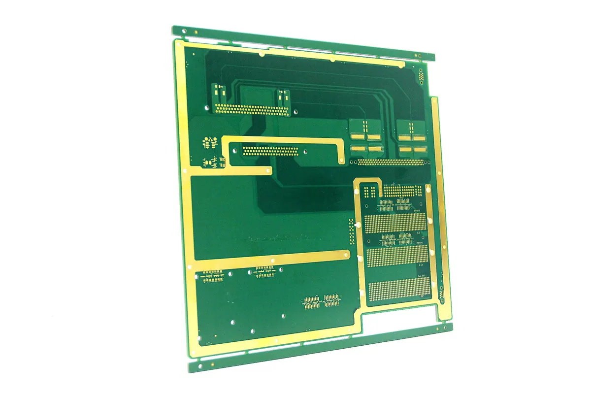
Heavy copper and power PCBs are essential for applications requiring high current handling, such as power supplies, motor drives, and automotive systems. These boards use copper weights of 3 oz/ft² or more to reduce resistance, manage thermal rise, and ensure reliable power distribution. However, the increased copper thickness introduces manufacturing challenges, including longer etch times, plating difficulties, and thermal stress risks. Success depends on careful design, material selection, and rigorous testing throughout the production process.
For Omini RFQs, heavy copper requirements should be reviewed through design for manufacturability (DFM), stackup planning, inspection scope, and test evidence before release.
Design Considerations for Heavy Copper PCBs
Designing heavy copper PCBs starts with understanding current requirements and thermal limits. Using IPC-2152, designers calculate appropriate trace widths and thicknesses to keep temperature rise within acceptable limits—typically 10°C for internal layers and 20°C for external layers under continuous load. For currents above 10A, 3 oz copper is often the minimum, with 6 oz or more used in high-power modules.
Copper balancing is critical to prevent warpage during lamination. Designers should mirror copper areas on opposite layers or use cross-hatched planes to maintain symmetry. Thermal reliefs on component pads reduce heat sinking during soldering, improving solder joint quality. Via design must account for increased current density; multiple vias in parallel or filled and plated vias help distribute current and reduce voltage drop.
Clearance between high-current traces and adjacent features must follow IPC-2221 standards to prevent arcing and ensure dielectric integrity. Designers should also consider the coefficient of thermal expansion (CTE) mismatch between copper and substrate, especially in multilayer builds, to avoid delamination during thermal cycling.
Manufacturing Challenges and Process Adjustments
Fabricating heavy copper PCBs requires adjustments to standard etching, plating, and lamination processes. Thicker copper increases etch time, which can lead to undercutting if not carefully controlled. The quote package should identify trace-width tolerance, copper weight, and acceptance evidence so the manufacturing route is clear before production.
Plating thick copper layers demands process control to support uniform deposition. For internal layers, the lamination process must accommodate thicker copper foils without causing resin starvation or voids. Prepreg selection and press-cycle assumptions should be reviewed during DFM.
Drilling through heavy copper presents challenges due to increased tool wear and burr formation. Plated through-holes (PTHs) in heavy copper boards may require longer plating time; thickness measurement or cross-section analysis should be specified when the via structure is reliability-critical.
Surface finish selection also matters. HASL can lead to uneven surfaces on thick copper, while ENIG or OSP may be preferred for flatness and solderability. For high-reliability applications, finish compatibility with assembly processes and environmental exposure should be reviewed before release.
Inspection and Testing for Quality Assurance
Given the complexity of heavy copper PCBs, inspection and testing are vital to detect defects that could compromise performance. Automated Optical Inspection (AOI) identifies surface defects such as shorts, opens, and missing features after etching and plating. The inspection plan should state which stages and records are required.
X-ray inspection is essential for evaluating internal features like via fill, plating voids, and delamination that are not visible optically. This is especially important for buried vias and high-density interconnect areas in power PCBs. X-ray helps confirm proper barrel thickness and detect inclusions or gaps.
In-Circuit Testing (ICT) verifies netlist continuity and isolation, catching opens and shorts in high-current paths. However, ICT may have limited access due to thick copper and large components. In such cases, flying probe testing can adapt to complex geometries without requiring custom fixtures. For more on this approach, see our guide on Demystifying Flying Probe PCB Testing: The What, Why, and How.
Functional testing under simulated load conditions can validate voltage regulation, current handling, and thermal performance when it is included in the agreed test scope. Traceability requirements should name the records needed for later root-cause analysis and customer approval.
Common Failure Modes and Prevention
Despite careful design, heavy copper PCBs can fail due to avoidable issues. Etch undercut reduces trace width, increasing resistance and risk of overheating. Plating voids in vias create open circuits under thermal stress. Delamination occurs when lamination is insufficient or CTE mismatch causes layer separation during cycling.
To prevent these, use DFM review during Gerber and BOM assessment. Designers should avoid sharp angles in traces, use teardrops at trace-to-pad connections, and ensure adequate annular rings. For detailed failure analysis and prevention strategies, refer to our resource on Common Failures in Heavy Copper PCB and How to Avoid Them in the Design Stage.
Thermal cycling tests and power-on burn-in can help validate long-term reliability when the customer requirement calls for that evidence.
Material Selection and Stackup Planning
Choosing the right substrate is as important as copper weight. FR-4 is common for moderate power applications, but for high thermal demands, materials like polyimide, PTFE, or metal-core PCBs (MCPCBs) offer better thermal conductivity and CTE matching. The RFQ should connect material choice to operating temperature, thermal cycling requirements, and dielectric properties.
Stackup symmetry remains crucial. Designers should balance copper weights across layers and use consistent prepreg types to prevent warpage. For boards with mixed copper weights—such as 6 oz power layers and 1 oz signal layers—careful planning is needed to manage differential etching and plating rates.
Copper infiltration into prepreg during lamination can affect dielectric thickness. Stackup review should account for resin flow, controlled impedance needs, and dimensional stability.
Applications Driving Heavy Copper Demand
Heavy copper and power PCBs are widely used in power conversion systems, including DC-DC converters, inverters, and battery chargers. Automotive applications such as electric vehicle (EV) onboard chargers, DC-DC converters, and motor controllers rely on heavy copper for high-current bus bars and power distribution.
Industrial motor drives, welding equipment, and power supplies for telecommunications infrastructure also benefit from reduced voltage drop and improved thermal management. In renewable energy systems, heavy copper PCBs support solar inverters and wind turbine converters where efficiency and reliability are paramount.
LED lighting, particularly high-power and flexible LED PCBs, often incorporates heavy copper for thermal management. For insights on flexible LED applications, see our article on Flexible LED PCBs: Advantages, Applications, and Design Considerations.
Connector interfaces, such as those in gold finger PCBs, may also use heavy copper to handle repeated insertion cycles and current loads. Learn more about gold finger implementations in our guide on Gold Finger PCBs: Types, Benefits, and Applications.
For complex designs requiring fine features alongside power layers, HDI techniques can be integrated. Explore tradeoffs and applications in our overview of HDI PCBs: Types, Advantages, Drawbacks, and Applications.
Final Notes from the Floor
Building reliable heavy copper PCBs requires more than just specifying thick copper; it demands attention to design symmetry, process control, and validation at every stage. Teams that treat copper weight as a system variable, rather than an isolated spec, reduce avoidable quote and production risk. Omini uses the RFQ review to connect these requirements to the manufacturing and quality evidence needed for the project.
> Engineering handoff note: How to Choose SMT AOI Inspection Coverage for PCB Assembly Defects before the release package is frozen.