
Direct Answer
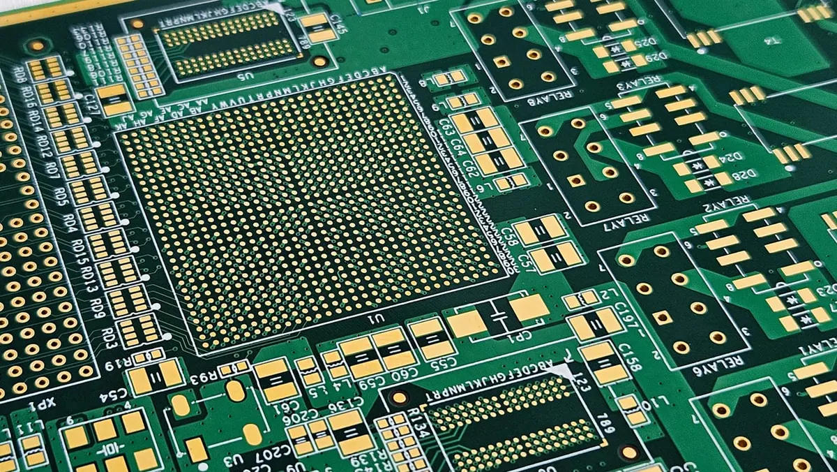
HDI PCBs, or High-Density Interconnect printed circuit boards, are engineered to pack more circuitry into smaller spaces using microvias, fine lines, and sequential lamination. Unlike standard multilayer boards that rely on through-hole vias, HDI designs use blind, buried, and stacked microvias to route signals between layers efficiently. This allows designers to reduce board size while increasing functionality—critical in devices where space is limited but performance demands are high.
These boards are not just about miniaturization; they directly impact signal integrity, power distribution, and thermal performance. By shortening signal paths and reducing via inductance, HDI technology supports high-speed interfaces like DDR, PCIe, and 5G RF. However, achieving these benefits requires tight process control during fabrication and assembly, making partnership with an experienced manufacturer essential.
Types of HDI PCB Structures
HDI technology is categorized by its via structure and build-up approach. The most common classifications are 1+N+1, 2+N+2, and 3+N+3, where N represents the number of core layers and the numbers indicate microvia layers on each side. A 1+N+1 HDI board has one microvia layer on top and bottom of a central core, suitable for moderate density increases. For higher complexity, 2+N+2 adds two microvia layers per side, enabling finer pitch BGAs and more routing channels.
Beyond layer count, via types define manufacturability. Blind vias connect an outer layer to an inner layer without going through the board. Buried vias link inner layers only, invisible from the surface. Stacked vias align multiple microvias vertically to span several layers, while staggered vias offset them to reduce stress. Each choice impacts drilling precision, plating reliability, and overall cost.
During RFQ, Gerber files and stack-up designs should be evaluated early so the HDI structure matches component pitch, signal integrity needs, and manufacturability constraints. This prevents costly redesigns later.
Advantages of HDI in Modern Electronics
The primary advantage of HDI is increased routing density without increasing board footprint. By using microvias as small as 75µm in diameter and line/space down to 75µm, designers can escape fine-pitch BGAs and QFNs that would be impossible on standard boards. This is especially valuable in smartphones, wearables, and medical implants where every millimeter counts.
Signal integrity improves significantly in HDI designs. Shorter trace lengths and reduced via stubs minimize signal reflection, crosstalk, and electromagnetic interference (EMI). For high-speed digital and RF applications, this means better eye margins and lower bit error rates. Power integrity also benefits from lower inductance in power delivery networks, reducing voltage droop under dynamic loads.
Thermal management sees indirect gains too. HDI allows for more efficient use of internal copper planes for heat spreading and enables thermal vias under components—though these are often formed as filled or plated microvias. In LED or power electronics applications, this helps maintain junction temperatures within safe limits.
Finally, HDI can reduce overall layer count. A function that might require 8 layers in a traditional design could be achieved in 6 layers with HDI, lowering material cost and simplifying lamination—though this benefit is often offset by increased process complexity.
Drawbacks and Manufacturing Challenges
Despite their benefits, HDI PCBs introduce significant manufacturing challenges. The drilling of microvias requires precise laser equipment; mechanical drills cannot achieve the needed size and aspect ratio. Laser drilling adds cost and demands tight control over pulse energy, focus, and debris cleanup to avoid defects like under-cutting or delamination.
Plating reliability is another concern. Microvias have high aspect ratios (depth-to-diameter), making uniform copper plating difficult. Poor plating can lead to open circuits or intermittent connections, especially under thermal cycling. To mitigate this, manufacturers use specialized electrolytes, pulse plating, or via filling with conductive or non-conductive paste followed by planarization.
Layer alignment becomes more critical with sequential lamination. Each build-up step must register precisely to previous layers; any shift causes layer-to-layer misalignment, risking opens or shorts. This drives up the need for high-precision lamination presses and optical registration systems.
Inspection also grows more complex. Standard AOI may miss microvia defects, so the inspection plan should define whether X-ray, cross-section, coupon, or electrical evidence is needed for via completeness, plating integrity, and internal layer registration.
Finally, cost and lead time increase. HDI boards typically cost 20-50% more than standard multilayers of similar size due to specialized equipment, materials, and process steps. Lead times extend by 3-5 days on average, depending on complexity. DFM consultation early in the design phase helps balance performance needs with manufacturability and budget.
Applications Across Industries
HDI PCBs are ubiquitous in consumer electronics. Smartphones use 2+N+2 or 3+N+3 structures to accommodate multi-core processors, advanced cameras, and 5G modems in thin form factors. Tablets and ultrabooks rely on HDI for similar reasons—high performance in limited space.
In medical devices, HDI enables implantable electronics like pacemakers and neurostimulators, where miniaturization and long-term reliability are critical. Diagnostic equipment such as ultrasound and portable MRI systems also benefit from HDI’s signal integrity and noise reduction.
Automotive applications are growing rapidly. Advanced driver-assistance systems (ADAS), lidar sensors, and infotainment units use HDI to manage high-speed data from cameras and radar while resisting vibration and temperature extremes. Here, IPC Class 3 compliance and rigorous testing (including thermal cycling and HAST) are standard.
Aerospace and defense systems leverage HDI for avionics, flight controls, and satellite payloads where size, weight, and performance are paramount. These applications often require project-specific approval evidence, conformal coating, hermetic sealing, and traceability to lot and batch levels.
Industrial equipment, including robotics and power inverters, uses HDI for compact motor drives and control boards. Even in less extreme environments, the reliability gains from shorter signal paths and reduced via failure modes contribute to longer field life.
Design for Manufacturability (DFM) and Process Control
Successful HDI production starts long before fabrication. DFM review checks for minimum annular ring, via-in-pad feasibility, solder mask sliver, and copper thinning risks. For via-in-pad designs, which are common in HDI to save space, the review should evaluate whether copper-filled or epoxy-filled vias with surface plating are needed to prevent solder wicking and support BGA assembly.
Panelization strategy affects yield. HDI panels often use smaller arrays with robust tooling edges and fiducials to maintain registration during sequential lamination. The panel layout should balance throughput with defect risk.
During SMT assembly, fine-pitch components demand precise solder paste printing and placement. SPI (solder paste inspection), AOI, and X-ray may be scoped when paste volume, placement accuracy, voids, solder bridging, or hidden joints create release risk.
Functional testing validates end-to-end performance. For high-speed HDI boards, this may include time-domain reflectometry (TDR) for impedance control or eye-pattern testing for signal integrity when the customer requires those records. Test coverage should match the design's operating environment.
Traceability is maintained throughout. Each panel receives a unique identifier tracked from Gerber input through final test, linking to inspection data, BOM versions, and operator logs. This supports root cause analysis if field failures occur and meets IPC and customer-specific audit requirements.
The Role of Inspection and Testing
Quality and reliability in HDI manufacturing hinge on advanced inspection. Standard optical inspection cannot detect internal via defects or buried layer issues. X-ray is essential for viewing microvia continuity, plating voids, and layer-to-layer registration—especially in stacked or staggered via structures.
An HDI inspection protocol may include:
- Post-drill X-ray to confirm laser drill quality and debris removal
- Post-plate X-ray to verify copper plating thickness and uniformity
- Post-lamination X-ray to check layer alignment and dielectric bonding
- Post-reflow X-ray (2D and 3D) for solder joint integrity under BGAs and QFNs
- AOI after each major step for surface defects like shorts, opens, and missing components
ICT and functional testing follow assembly when required. For HDI boards with high node density, flying probe or custom fixture ICT can test netlist continuity and isolation. Functional tests should replicate the operating conditions that matter for customer acceptance.
Inspection records should be linked to traceability requirements when the buyer needs later trend analysis, root-cause review, or supplier approval evidence.
Partnering for HDI Success
Choosing the right manufacturing supplier is as important as the design itself. HDI success depends on verified laser drilling, sequential lamination, plating control, and inspection capability. Buyers should confirm these items against the actual project stackup and evidence needs.
From initial Gerber/BOM review to final shipment, the Omini RFQ path should make stack-up, via structure, material selection, performance, cost, lead time, process validation, first-article inspection, and traceability assumptions visible before release.
For companies developing next-generation electronics in computing, communications, medical, or automotive sectors, HDI is often unavoidable. Its complexity becomes manageable when DFM, IPC expectations, traceability, and inspection scope are defined before production.
As electronic devices continue to shrink while demanding more from their circuitry, HDI will remain a key enabler. Understanding its types, trade-offs, and application fit allows designers to make informed decisions. And by engaging early with a manufacturing partner that respects both design intent and process reality, teams can avoid costly surprises and bring reliable, high-density products to market faster.
Related Omini Engineering Notes
- Flexible LED PCBs: Advantages, Applications, and Design Considerations
- Gold Finger PCBs: Types, Benefits, and Applications
- Flex Circuit Boards: Introduction and Applications: Introduction and Applications
- AOI and X-Ray Inspection in PCB Assembly
- Double Sided PCB: Advantages, Applications, and Manufacturing Process
Related Omini Engineering Notes
> Engineering handoff note: How to Choose SMT AOI Inspection Coverage for PCB Assembly Defects before the release package is frozen.