
Direct Answer
LED PCB design succeeds when thermal, electrical, and manufacturing constraints are balanced from the first layout decision. A well-designed LED board keeps junction temperatures below datasheet limits, delivers consistent current to every emitter, and passes through fabrication and assembly without rework. This requires metal-core substrates or thermal via arrays, correctly sized copper traces, constant-current driver topology, and DFM verification before release. Engineers who prioritize these four areas produce lighting solutions with predictable brightness, color stability, and service life.
Thermal Management: The First Priority in LED PCB Design
Thermal management determines whether an LED PCB will perform reliably or fail prematurely. LEDs convert only a fraction of electrical energy into light; the remainder becomes heat that must be conducted away from the semiconductor junction. If junction temperature exceeds the manufacturer's maximum rating, light output decreases, color shifts toward longer wavelengths, and lifetime drops dramatically. The PCB is the primary heat path, so its thermal design directly controls system reliability.
Metal-Core PCBs vs. FR4 with Thermal Vias
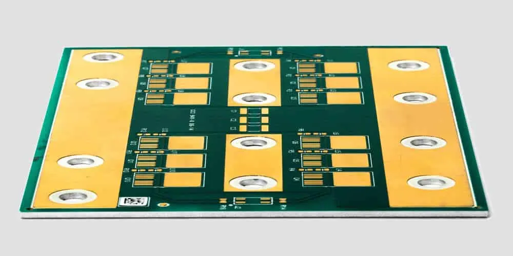
The most effective thermal solution is a metal-core PCB (MCPCB), which uses an aluminum or copper base plate with a thermally conductive dielectric layer. Typical MCPCB constructions use 1.0 mm to 3.2 mm aluminum bases with dielectric thermal conductivities ranging from 1 W/m·K to 3 W/m·K. Copper-base MCPCBs offer even higher thermal performance but cost significantly more. For high-power LEDs operating above 1 W per emitter, an MCPCB is usually the correct choice.
For lower-power applications or prototyping on standard FR4, thermal via arrays under the LED pad provide an alternative. A typical thermal via pattern uses 0.3 mm drilled vias on a 0.8 mm pitch, filled or tented with thermally conductive material. The vias conduct heat from the top-layer pad through the board to a copper pour on the bottom layer, which can then attach to a heatsink. However, FR4's low thermal conductivity (approximately 0.2 W/m·K to 0.4 W/m·K) means that even with vias, thermal resistance remains significantly higher than an MCPCB. Use FR4 with thermal vias only when power dissipation is modest and the ambient temperature is controlled.
Copper Weight and Heat Spreading
Copper weight directly affects both electrical current capacity and lateral heat spreading. Standard 1 oz (35 µm) copper is often insufficient for LED boards carrying more than 1 A per trace. For high-current LED circuits, specify 2 oz (70 µm) or 3 oz (105 µm) copper on the top layer. The thicker copper spreads heat laterally from the LED pad before it reaches the thermal vias or dielectric layer, reducing the effective thermal resistance of the entire stackup.
The thermal pad under each LED should be as large as the component footprint allows. For SMD packages like 5050 or 3030, the datasheet typically specifies a recommended pad pattern that includes a large exposed thermal pad. Extend this pad with a copper pour that connects to thermal vias or the MCPCB dielectric. Avoid placing thermal vias directly under the LED pad if solder wicking is a concern; instead, use filled or capped vias to prevent solder from flowing into the via barrel during reflow.
> Practical note: When using thermal vias on an FR4 board, specify via-in-pad with conductive fill or tented vias on the back side. Unfilled vias under an LED pad will wick solder away from the joint during reflow, creating voids that increase thermal resistance and weaken the solder connection.
Current Control and Trace Sizing for Consistent Brightness
LED brightness is directly proportional to forward current, and even small current variations between LEDs in the same string cause visible brightness differences. Current control starts with the driver topology and continues through PCB trace design. A constant-current driver is mandatory for LED circuits; voltage-regulated supplies cannot compensate for the exponential current-voltage relationship of LEDs, where a small voltage change produces a large current change.
Trace Width Calculation for LED Current
Trace width must be sized for both the steady-state current and the acceptable temperature rise. IPC-2221 provides the framework for calculating trace current capacity based on cross-sectional area and allowable temperature rise. For a 1 A LED string on 1 oz copper, a trace width of at least 0.5 mm is typical for a 10 °C temperature rise. At 2 A, the trace width should increase to approximately 1.5 mm on the same copper weight. These values assume external traces with natural convection cooling; internal layers require wider traces because heat dissipation is poorer.
Trace resistance also matters for voltage drop and brightness uniformity. A 100 mm trace of 0.5 mm width on 1 oz copper has approximately 0.1 Ω of resistance. At 1 A, this drops 100 mV, which can be significant in a low-voltage LED string. If multiple LEDs share a common power trace, the LED farthest from the power input receives less voltage and therefore less current, producing uneven brightness. Use star routing or a power plane to equalize trace lengths and resistance to each LED or LED group.
Constant-Current Driver Placement
The constant-current driver should be placed close to the LED array to minimize trace length between the driver output and the LEDs. Long traces between driver and LED add parasitic resistance and inductance, which can cause current instability, especially in pulse-width-modulated dimming applications. Keep the high-current loop between the driver output capacitor and the LED string as short and tight as possible.
For multi-channel designs, each channel should have its own current-sense resistor placed close to the driver IC. The sense resistor's tolerance directly affects current accuracy; use 1% tolerance resistors for consistent brightness across channels. The Kelvin connection for the sense resistor—separate traces for the sense lines and the power path—prevents voltage drops in the power trace from corrupting the current measurement.
Design for Manufacturability: Rules That Prevent Rework
A thermally and electrically sound LED PCB still fails if it cannot be fabricated and assembled reliably. Design for manufacturability (DFM) rules for LED boards address spacing, pad patterns, thermal reliefs, and solder mask considerations. Following these rules during layout prevents costly rework and assembly yield losses.
Spacing and Clearance per IPC-2221
IPC-2221 defines minimum conductor spacing based on voltage and environmental conditions. For LED PCBs operating at low voltage (under 50 V), the minimum spacing is typically 0.1 mm for external layers under normal conditions. However, practical manufacturing limits often require larger spacing. Most PCB manufacturers prefer a minimum trace-to-trace spacing of 0.15 mm to 0.2 mm for reliable etching, and 0.2 mm to 0.25 mm for trace-to-pad spacing. Check your manufacturer's capability table before finalizing the layout.
For high-voltage LED drivers that operate from mains power (e.g., 120 VAC or 240 VAC), spacing requirements increase substantially. Creepage distances of 2 mm to 6 mm may be required depending on the pollution degree and the insulation class. These requirements affect both the PCB layout and the component placement, so they must be considered early in the design process.
Thermal Reliefs for Solderability
Thermal reliefs are small spokes that connect a pad to a copper pour, limiting heat flow from the pad to the pour during soldering. Without thermal reliefs, the copper pour acts as a heat sink that prevents the solder from reaching reflow temperature, causing cold joints or tombstoning. For LED PCBs with large ground or power planes, every through-hole pad and SMD pad that connects to a plane should have a thermal relief.
The standard thermal relief uses four spokes, each approximately 0.25 mm wide, with a clearance of 0.25 mm to 0.5 mm between the pad and the surrounding copper. For high-current connections, increase the spoke width to maintain current capacity while still limiting heat flow. Some designers remove thermal reliefs on high-current pads to reduce resistance, but this creates soldering problems. A better approach is to use multiple vias in parallel for high-current connections, each with its own thermal relief.
Solder Mask and Silkscreen Considerations
Solder mask openings should match the pad pattern exactly, with no mask slivers between adjacent pads. For fine-pitch LED packages, specify solder mask defined (SMD) pads or non-solder mask defined (NSMD) pads consistently. NSMD pads are generally preferred for SMT LEDs because the pad size is determined by the copper etch, which is more accurate than the solder mask opening. However, NSMD pads require a mask clearance of at least 0.075 mm around each pad.
Silkscreen should not overlap any solder pad or thermal pad. For LED polarity marking, use a clear diode symbol or a "cathode bar" on the silkscreen near the cathode pad. This is especially important for LEDs, where reversed polarity is a common assembly error that damages components during testing.
Assembly Process Considerations for SMT LED Packages
The assembly process for LED PCBs requires attention to pad patterns, solder paste application, and reflow profiling. SMT LED packages come in a range of sizes—from small 0402 packages to large 7070 packages—and each has specific assembly requirements. The pad pattern must match the package's solderable area exactly to ensure proper self-alignment during reflow.
Pad Pattern Design for SMD LEDs
The pad pattern for an SMD LED should follow the manufacturer's recommended footprint, which is typically provided in the datasheet. For packages with a thermal pad, the pad pattern must include a thermal pad of the correct size, connected to thermal vias or the MCPCB dielectric. The solder paste stencil aperture for the thermal pad should be approximately 50% to 75% of the pad area, using a grid of smaller apertures rather than one large opening. This prevents solder voiding and ensures consistent solder joint thickness.
For packages with side terminals, such as 2835 or 5630 LEDs, the pad pattern should extend slightly beyond the package body to allow solder fillet formation. A typical rule is to extend the pad 0.3 mm to 0.5 mm beyond the package edge. The pad width should match the terminal width or be slightly wider, but not so wide that adjacent pads risk solder bridging.
Reflow Profile and Thermal Considerations
LED packages have maximum reflow temperature ratings that must be respected during assembly. Most SMD LEDs are rated for a peak reflow temperature of 245 °C to 260 °C, but some high-power packages have lower ratings. The reflow profile must be set to achieve good solder wetting without exceeding the LED's peak temperature rating. A typical lead-free profile uses a ramp rate of 1 °C to 3 °C per second, a soak zone at 150 °C to 200 °C for 60 to 120 seconds, and a peak temperature of 235 °C to 245 °C for 20 to 40 seconds above liquidus.
The thermal mass of the PCB affects the reflow profile significantly. A metal-core PCB absorbs more heat than an FR4 board of the same size, so the reflow profile may need adjustment to ensure all pads reach the required temperature. Work with your assembly partner to develop a profile specific to your board's stackup and component mix. For boards with both LEDs and other SMT components, the profile must accommodate the most temperature-sensitive component.
Inspection and Testing After Assembly
After reflow, LED PCBs require inspection to verify solder joint quality and correct polarity. Automated optical inspection (AOI) can detect missing components, reversed polarity, and solder defects such as bridging or insufficient solder. For LED boards, AOI should include a polarity check using the silkscreen marks or the package's visual polarity indicator.
Electrical testing should include a forward voltage test for each LED or LED string. This test verifies that the LEDs are correctly oriented and that the current path is continuous. A simple continuity test is insufficient because it does not verify polarity. For boards with multiple LED strings, test each string independently to identify any assembly defects before the board is integrated into the final product.
Common Mistakes and How to Avoid Them
Engineers designing LED PCBs often repeat the same mistakes, which range from minor performance issues to complete board failures. Recognizing these errors early in the design process saves time, money, and rework cycles.
Undersizing Copper Traces
The most common mistake is undersizing copper traces for the expected current. A trace that is too narrow heats up, increasing resistance and causing a voltage drop that reduces LED brightness. In extreme cases, the trace can overheat and delaminate from the substrate. Always calculate trace width using the maximum expected current, including any inrush current at power-on, and add a safety margin of at least 25%.
Ignoring Solder Joint Thermal Resistance
The solder joint between the LED pad and the PCB thermal pad is part of the thermal path. A thin or voided solder joint has higher thermal resistance than a full, void-free joint. Solder voids are particularly problematic on large thermal pads. Using a stencil with multiple smaller apertures instead of one large opening reduces voiding. Also, ensure that the solder paste is fresh and properly stored, as oxidized paste increases voiding.
Placing LEDs Too Close Together
LEDs placed too close together create localized hot spots that exceed the thermal design limits. The heat from adjacent LEDs accumulates, raising the junction temperature of each LED above the calculated value. Maintain a minimum spacing between LEDs based on the thermal simulation or the MCPCB's heat spreading capability. For high-power LEDs, a spacing of at least 5 mm to 10 mm is typical, but this depends on the specific package and power level.
Forgetting Thermal Reliefs on Ground Pads
Ground pads connected directly to a large copper pour without thermal reliefs cause soldering defects. The pour conducts heat away from the pad, preventing the solder from reaching reflow temperature. This results in cold joints, tombstoning, or incomplete wetting. Always add thermal reliefs to ground and power pads, even if it means slightly increasing the pad's electrical resistance.
Not Accounting for Voltage Drop Across Long Traces
Long traces between the power supply and the LEDs cause voltage drops that reduce brightness and create uneven illumination. This is especially problematic in LED strips or boards with LEDs distributed over a large area. Use wider traces or a power plane to minimize resistance, and consider using multiple supply points for long LED arrays.
Verifying Your Design Before Fabrication
Before sending your LED PCB design to fabrication, perform a thorough design review that covers thermal, electrical, and manufacturing aspects. This review catches errors that would otherwise result in expensive rework or failed boards.
DFM Review Checklist
Run a DFM review using your CAD tools or your manufacturer's online DFM checker. Verify that trace widths meet current-carrying requirements, that clearances comply with IPC-2221, and that thermal pads have proper via patterns. Check that all components have complete footprints and that no silkscreen overlaps pads. Review the solder mask openings to ensure they match the pad patterns.
For LED-specific checks, verify that each LED's thermal pad connects to the thermal management structure (MCPCB dielectric or thermal vias) without any thermal barrier. Confirm that the polarity markings are correct and consistent across the board. Check that the constant-current driver's sense resistor is placed correctly and that the Kelvin sense traces are properly routed.
Thermal Simulation and Testing
If possible, perform a thermal simulation of the LED PCB using finite element analysis (FEA) software. Input the LED power dissipation, the PCB stackup thermal properties, and the ambient temperature to calculate junction temperatures. Compare the results with the LED datasheet's maximum junction temperature. If the simulated junction temperature exceeds the limit, increase copper weight, add more thermal vias, or switch to an MCPCB.
For critical designs, build a prototype and measure the actual junction temperature using a thermal camera or a thermocouple attached to the LED case. This measurement validates the simulation and provides confidence before committing to production.
Preparing Complete Fabrication Files
When you are ready to order, provide complete fabrication files that include the Gerber files, drill files, and a detailed BOM with manufacturer part numbers. Specify the PCB stackup, including the substrate material, copper weight, and surface finish. For MCPCBs, specify the base metal thickness and the dielectric thermal conductivity. Include any special tolerances or test requirements in the fabrication notes.
For the RFQ, include the expected current per LED, the ambient operating temperature range, and whether you need thermal simulation or testing. This information helps the manufacturer provide an accurate quote and identify potential issues before fabrication begins. A complete and accurate RFQ reduces the risk of miscommunication and ensures that the manufacturer can produce your board exactly as intended.
When to Involve Your Manufacturing Partner
Involving your PCB manufacturer early in the design process prevents costly mistakes and improves the final product. Manufacturers have practical knowledge of fabrication limits, material availability, and assembly processes that can inform your design decisions.
Design Review Collaboration
Share your preliminary layout with your manufacturer before finalizing the design. They can identify potential fabrication issues, such as minimum trace spacing that is too tight for their process, via sizes that are not drillable, or thermal reliefs that are too narrow. This review is especially important for MCPCBs, where the dielectric layer and base metal thickness affect both thermal performance and manufacturability.
For complex designs, consider a design-for-manufacturing session where your engineering team and the manufacturer's process engineers review the layout together. This collaboration can uncover issues that automated DFM checks miss, such as thermal pad patterns that are not compatible with the assembly process or component placements that complicate testing.
Material Selection and Stackup Advice
Your manufacturer can advise on material selection based on your thermal and electrical requirements. For MCPCBs, they can recommend specific dielectric materials based on thermal conductivity and cost. For FR4 boards, they can advise on the appropriate copper weight and via fill options. They can also provide guidance on surface finish selection—ENIG is often preferred for SMD LEDs due to its flat surface and good solderability, while HASL may be acceptable for through-hole designs.
Assembly Process Coordination
If you are using a PCBA service, coordinate the assembly process with your manufacturer. They can provide recommendations for stencil design, reflow profiles, and inspection methods based on your component mix. For LED boards with mixed SMT and through-hole components, they can advise on the optimal assembly sequence to minimize thermal stress on the LEDs.
Omini offers integrated PCB fabrication and assembly services, allowing you to work with a single partner from design review through final testing. This integration ensures that the fabrication and assembly processes are optimized together, reducing lead times and improving yield. For engineers designing LED PCBs, partnering with a manufacturer that understands both the thermal and assembly challenges of LED lighting is essential for producing reliable, efficient products.
For engineers new to PCB design, reviewing fundamental guidelines can prevent basic errors before they reach the manufacturer. The PCB Design Guidelines for Beginners: Rules and DFM Checklist provides a solid foundation for design rules and DFM practices. For more advanced designs, such as those with dense component placement or high-speed driver circuits, the HDI PCB Design: Comprehensive Guidelines, Process and Considerations article covers the additional constraints of high-density interconnect technology.
If your LED design requires flexible substrates, such as for LED strips or wearable lighting, the Flex PCB Manufacturing Process: An Overview for Beginners explains the unique considerations of flexible circuits. For LED drivers operating at high frequencies, the Controlled Impedance PCB Design Rules for Reliable Fabrication article addresses the impedance control requirements that affect driver performance. Finally, understanding the SMT assembly process helps you design for efficient and reliable assembly of your LED PCBs.
Frequently Asked Questions
Why is thermal management so important in LED PCB design?
LEDs generate heat that must be conducted away from the junction. If the junction temperature exceeds the datasheet maximum, light output drops, color shifts, and lifespan shortens. Using a metal-core PCB (MCPCB) or a thermal via array under the LED pad helps transfer heat to a heatsink or the ambient environment. The PCB is the primary heat path, so its thermal design directly controls system reliability.
What are common mistakes engineers make when designing LED PCBs?
Common mistakes include undersizing copper traces for the expected current, ignoring the thermal resistance of the solder joint, placing LEDs too close together without adequate heat spreading, and forgetting to add thermal reliefs on ground pads, which makes soldering difficult. Not accounting for the voltage drop across long traces can also cause uneven brightness across the LED array.
How can I verify my LED PCB design before fabrication?
Perform a design for manufacturability (DFM) review using your CAD tools or your manufacturer's DFM check. Verify that trace widths meet current-carrying requirements, that clearances comply with IPC-2221, and that thermal pads have proper via patterns. Simulate thermal performance if possible, and review the Gerber files and stackup with your manufacturer before placing the order.
What information should I include in an RFQ for an LED PCB?
Include the complete Gerber files, a detailed BOM with manufacturer part numbers, the PCB stackup (especially if using a metal-core board), the required copper weight, surface finish, and any special tolerances. Specify the expected current per LED, the ambient operating temperature, and whether you need thermal simulation or testing. This helps the manufacturer provide an accurate quote and identify potential issues.
How does the choice of surface finish affect LED PCB assembly?
Surface finish impacts solderability and reliability. For LED PCBs, ENIG (electroless nickel immersion gold) is often preferred because it provides a flat surface for SMD LEDs and good solder joint integrity. HASL can be acceptable for through-hole LEDs but may not be flat enough for fine-pitch SMD components. The finish also affects the thermal resistance of the solder joint.
What is the role of the PCB stackup in LED lighting design?
The stackup determines the thermal path and electrical performance. A metal-core PCB (MCPCB) uses a thermally conductive dielectric layer over an aluminum or copper base to spread heat efficiently. For FR4 boards, a thicker copper layer (e.g., 2 oz or more) and thermal vias can improve heat dissipation. The stackup also affects impedance for high-speed LED drivers, so it must be specified correctly.
> Engineering handoff note: Low-Cost PCB Manufacturing: Maximising Value Without Sacrificing Quality before the release package is frozen.