
Direct Answer
Programming a printed circuit board doesn’t mean writing software for the board itself—it means preparing the manufacturing data that tells automated equipment how to build, inspect, and test it. In an EMS environment, this process translates design outputs like Gerbers and BOMs into machine instructions for SMT placement, AOI, X-ray, and functional test systems. The goal is to convert a circuit design into a repeatable, high-yield production process.
This step is often overlooked by engineers focused on schematic capture and layout, but incomplete or incorrect programming data is a leading cause of assembly delays, tombstoning, misalignments, and false test failures. A well-executed programming workflow catches these issues early, saving time and cost.
Gerber and BOM Validation: The Foundation
The first step in PCB programming is validating the Gerber files and bill of materials (BOM). Gerbers define the copper layers, solder mask, silkscreen, and drill holes—any error here means the physical board won’t match the design. The BOM must list every component with correct MPN, reference designator, quantity, and package type. Mismatches between BOM and schematic or layout are common, especially when last-minute substitutions occur.
At Omini, we run automated Gerber checks against IPC-2581 standards and cross-reference the BOM with the centroid data to ensure every part has a valid footprint and placement coordinate. We also verify polarity markers for diodes, LEDs, and ICs—silkscreen errors here can lead to 180-degree reversals during SMT. This step alone prevents up to 70% of avoidable assembly defects.
DFM Analysis: Designing for Real-World Production
Once the data is clean, we perform Design for Manufacturing (DFM) analysis. This isn’t just about checking trace width or clearance—it’s about ensuring the design can be reliably assembled, inspected, and tested at volume. For example, we check for:
- Solder mask slivers between fine-pitch pads that could cause bridging
- Component placement too close to board edges, risking damage during depaneling
- Via-in-pad designs without proper capping, which can trap solder or create voids
- Test point accessibility for ICT or probe fixtures
If a BGA has insufficient escape routing or a QFN lacks adequate thermal vias, we flag it early. These aren’t always design errors—they’re often oversights in high-density layouts—but they directly impact yield and reliability. Addressing DFM comments before SMT programming avoids costly stencil changes or rework loops.
SMT Programming: From Data to Machine Instructions
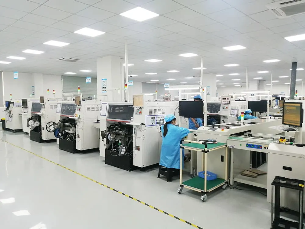
With validated Gerbers, BOM, and centroid data, we generate the SMT placement program. This file tells the pick-and-place machine exactly where each component goes, its rotation, and the nozzle type to use. We also generate solder paste stencil data based on paste volume calculations and aperture sizing rules—critical for avoiding insufficient solder on BGAs or excess solder on 0201 passives.
We use Siemens SiPlace and Yamaha YSM series machines, which require specific formats like .csv or .txt centroid files with X/Y coordinates, rotation, and part number. Our engineers review the placement simulation to check for collisions, especially with tall components like electrolytic capacitors or transformers near the board edge. We also verify that fiducial marks are correctly placed and detectable under machine vision—poor fiducials are a silent cause of placement drift.
AOI and X-Ray Programming: Building Inspection into the Process
Automated Optical Inspection (AOI) and X-ray inspection aren’t afterthoughts—they’re programmed alongside SMT. For AOI, we define inspection zones, expected solder joint shapes, and component polarity checks. For example, we program the system to flag reversed LEDs or missing passives based on contrast and shape recognition.
For BGAs, QFNs, or LGAs, X-ray is essential. We program the X-ray system to inspect solder joint voids, shorts, and opens using laminography or tilted-beam techniques. Parameters like kV, mA, and exposure time are tuned per package type—too much radiation can damage sensitive components, too little misses defects. Omini’s X-ray programs are qualified using IPC-A-610 Class 2 and Class 3 acceptance criteria.
Functional Test Programming: Verifying Real-World Behavior
After assembly, the PCBA must be tested to confirm it works as intended. Functional test programming involves creating a test sequence that powers the board, applies stimuli (signals, voltages, loads), and measures responses. This might include:
- Power-up sequencing and inrush current monitoring
- Digital interface handshakes (I2C, SPI, UART)
- Analog signal chain validation (gain, offset, bandwidth)
- Boundary scan (JTAG) for interconnect testing
We develop these test programs using platforms like NI TestStand or custom Python scripts, often integrating with the customer’s existing test fixtures. The test program must be repeatable, safe, and fast—targeting under 30 seconds per board for high-volume runs. We also include diagnostic logging to help identify failure modes during early production.
First Article Inspection and Feedback Loop
Before full production, we run a first article inspection (FAI). This includes visual checks, AOI, X-ray, and functional test on the first 5–10 boards. Any discrepancies between expected and actual results trigger a feedback loop—sometimes the issue is in the programming data (e.g., wrong centroid rotation), sometimes it’s a component substitution issue, or a stencil defect.
We document all findings and update the programming files if needed. This iterative step ensures that when we scale to 1,000 or 10,000 units, the yield remains high and false rejects stay low. It’s also where we validate that the test program catches real defects—not just nuisance trips.
Why Partner with an EMS Provider for PCB Programming?
Many OEMs try to handle PCB programming in-house using free tools or outdated scripts, but this often leads to inconsistent results. An experienced EMS provider like Omini brings calibrated equipment, qualified engineers, and a proven workflow that ties Gerber validation, DFM, SMT setup, inspection, and test into a single coherent process.
We’ve seen cases where a customer’s internal programming missed a silkscreen polarity mark, causing 200 boards to be assembled with reversed ICs—caught only after functional test failed. With proper EMS oversight, that error would have been flagged during Gerber review or AOI programming.
The bottom line: PCB programming isn’t just about file conversion—it’s about risk reduction, yield protection, and ensuring that what you designed is what gets built and tested. When done right, it’s invisible. When done poorly, it shows up in every batch.
Related Omini Engineering Notes
- Circuit Board Manufacturing Process: A Comprehensive Guide for Beginners
- Comparing Different Types of Printed Circuit Board Materials
- Electronics Manufacturing Process: A Comprehensive Guide
- Best EMS Companies in China 2026
- Fast Turn Printed Circuit Board Assembly: A Game-Changer for Your Business
> Engineering handoff note: How to Plan IC Substrate and Advanced Packaging Supply Chain Risk before the release package is frozen.
> Engineering handoff note: How to Evaluate PCB Supply Chain Risk from AI Server and Automotive Trends before the release package is frozen.
> Engineering handoff note: How to Evaluate PCB Supply Chain Risk from Automotive and Automotive Electronics Trends before the release package is frozen.