
Réponse directe
Evaluate SMT assembly risk by auditing circuit symbol-to-footprint consistency, BOM accuracy, and centroid generation before sending files to your PCBA partner. Symbol errors propagate into footprint pad mapping, netlist integrity, and pick-and-place programming, causing tombstoning, opens, and misaligned components. Review pin names, polarity markers, thermal pad connections, and package revisions against the datasheet to catch defects before fabrication.
Why Circuit Symbols Drive SMT Assembly Risk
Circuit symbols are not decorative placeholders. They carry the logical intent that becomes the physical footprint, the netlist, and ultimately the assembly data your manufacturer uses to place components. When a symbol contains an error, that error propagates through the entire design chain.
The connection between symbol and assembly risk is direct. A symbol that hides pin polarity, omits thermal pad connections, or assigns incorrect net classes produces a footprint that does not match the physical package. That mismatch leads to poor wetting, tombstoning, opens, or shorts. The cost of catching these issues during design review is a few hours of engineering time. The cost of catching them after stencil fabrication and solder paste printing is a respin and a delayed prototype.
Engineers often treat the schematic symbol as a purely logical element, ignoring its link to the footprint. This is the root cause of most SMT assembly failures traced back to design data. The symbol defines pin names, pin numbers, and pin functions. The footprint defines pad locations, pad sizes, and pad numbers. If these two do not align, the netlist will not match the physical board, and the centroid file will not match the BOM.
Review the symbol against the datasheet before you place a single component. Check pin 1 orientation, pin count, and thermal pad assignment. Confirm that the symbol revision matches the footprint revision in your library. A shared library with mismatched revisions is a silent killer.
Symbol-to-Footprint Consistency: The First Risk Filter
The first and most important evaluation step is comparing the schematic symbol to the PCB footprint. This is not a visual check; it is a data integrity check that must be performed systematically.
Pin Mapping and Pin Count Verification
Open the symbol properties and the footprint properties side by side. Verify that the number of pins in the symbol equals the number of pads in the footprint. This sounds trivial, but it is the most common source of assembly risk.
A QFN-32 package, for example, has 32 perimeter pads plus one exposed thermal pad. If the symbol only defines 32 pins and omits the thermal pad, the footprint will lack the center pad. The component will still be placed, but the thermal pad will not be soldered. This causes poor thermal dissipation, mechanical weakness, and potential electrical failure if the thermal pad is meant to be grounded.
Check pin names against the datasheet. A symbol that uses generic names like PAD1, PAD2, or NET1 instead of VCC, GND, or specific signal names will pass the schematic check but fail during layout review. The netlist will be ambiguous, and the assembler will not be able to verify connections during first-article inspection.
Polarity and Pin 1 Orientation
Polarity markers are critical for diodes, capacitors, LEDs, and connectors. A symbol with an incorrect polarity marker produces a footprint with mirrored orientation. The component will be placed backward, and the board will not function.
Verify pin 1 orientation in the symbol against the footprint and the datasheet. The pin 1 marker on the silkscreen must match the physical package. For BGA packages, the ball A1 location is defined by the datasheet. If the symbol maps ball A1 to the wrong corner, every ball will be shifted, and the component will not align with the pads.
Thermal Pad Connections
For QFN, BGA, and other packages with exposed thermal pads, the symbol must define the thermal pad net. This is often a separate pin in the symbol that connects to ground or a dedicated thermal net.
If the thermal pad is not defined in the symbol, the footprint will have a floating pad. The assembler will not know whether to connect it to ground, and the stencil aperture may not be designed for proper paste coverage. This leads to voids, poor thermal performance, and potential opens that are only detectable by X-ray inspection.
> Practical rule of thumb: Before layout, run a design rule check that compares symbol pin count and pin names against footprint pad count and pad numbers. This catches 80% of symbol-to-footprint mismatches before they become assembly failures.
BOM Accuracy and Reference Designator Integrity
The bill of materials is the bridge between your schematic and the assembler's procurement and placement process. A BOM with mismatched reference designators, incorrect manufacturer part numbers, or missing package types will stop the assembly line.
Cross-Checking BOM Against Schematic
Generate the BOM from the schematic, not from memory or a spreadsheet. Cross-check every reference designator against the schematic. A missing or duplicated reference designator will cause the assembler to reject the BOM or place the wrong component.
Verify that the package type in the BOM matches the footprint on the PCB. A BOM that lists a 0402 resistor when the footprint is 0603 will cause the assembler to reject the component during kitting. This is a simple check that prevents costly delays.
Manufacturer Part Numbers and Alternates
Include manufacturer part numbers in the BOM, not just generic descriptions. The assembler needs to source the exact component with the correct package, tolerance, and temperature rating. A BOM that lists "10k resistor" without a manufacturer part number forces the assembler to make assumptions, which increases risk.
If you have approved alternates, list them with their own manufacturer part numbers. Do not leave the alternates to the assembler's discretion unless you have a formal agreement.
Moisture Sensitivity and Handling
Components with moisture sensitivity levels above MSL 2 require special handling. The BOM should note MSL levels for each component, especially for BGA and QFN packages. J-STD-020 defines the classification and reflow profiles, while J-STD-033 covers handling, packing, and shipping.
If the BOM does not include MSL information, the assembler may bake components unnecessarily or skip baking when it is required. Both scenarios add risk. Baking components that do not need it wastes time; skipping baking for moisture-sensitive components causes popcorning during reflow.
Centroid File Generation and Verification
The centroid file, also called the pick-and-place file, tells the assembler where to place each component. It contains reference designators, X-Y coordinates, rotation, and the side of the board. Errors in the centroid file cause components to be placed in the wrong location or with the wrong orientation.
Generate from Layout, Not Schematic
The centroid file must be generated from the PCB layout, not from the schematic. The layout contains the actual pad positions and orientations. The schematic only contains logical connections.
Export the centroid file from your PCB design tool after the layout is complete and the design rule check passes. Verify that the file includes all components on both the top and bottom sides. A centroid file that omits bottom-side components will cause the assembler to miss those placements.
Verify Against BOM and Footprint
Cross-check the centroid file against the BOM. Every reference designator in the BOM must appear in the centroid file, and vice versa. A mismatch indicates a missing or duplicated component.
Check the rotation values in the centroid file against the footprint orientation. A rotation error of 90 degrees will place the component perpendicular to the pads, causing opens or shorts. This is especially critical for polarized components like diodes and electrolytic capacitors.
Coordinate System Consistency
Confirm that the centroid file uses the same coordinate system as the Gerber files. Most assemblers use the bottom-left corner as the origin, but some tools use the top-left or center. A coordinate system mismatch will shift every component by a fixed offset, causing a systematic placement error.
Include the coordinate system information in your RFQ or readme file. The assembler can then verify the alignment before running the pick-and-place machine.
DFM Review and RFQ Package Requirements
A meaningful DFM review requires complete and accurate data. The assembler needs more than just Gerber files to evaluate SMT assembly risk.
Required Files for RFQ
Incluez les éléments suivants dans votre package RFQ :
- Schematic PDF for reference and netlist verification
- Final BOM with manufacturer part numbers, package types, and MSL levels
- Centroid file in X-Y coordinates with rotation and side information
- Gerber or ODB++ files with complete layer stackup
- Fabrication drawing with board thickness, copper weight, and surface finish
- Any special requirements such as via-in-pad, edge plating, or impedance control
The assembler uses these files to run a DFM review that flags risks like missing thermal reliefs, incorrect stencil apertures, or insufficient solder mask clearance.
What the DFM Review Covers
The DFM review evaluates the PCB design against assembly process capabilities. It checks pad sizes and spacing against stencil design rules, verifies that components have adequate clearance for pick-and-place nozzles, and confirms that the board panelization is compatible with the assembly process.
The review also checks the BOM for component availability and alternate sourcing. If a component is obsolete or has a long lead time, the assembler can flag it before you commit to a build.
Quand impliquer le fabricant
Involve the manufacturer early, not after the design is locked. Send your files for a DFM review before you finalize the layout. This is especially important for complex packages like BGA, QFN, and fine-pitch components.
The manufacturer can provide feedback on stencil design, paste release, and reflow profile based on your specific board stackup and component mix. This feedback is more valuable before the design is frozen than after.
For related risk evaluation across different manufacturing contexts, review how FOPLP and thermal processing trends affect SMT assembly risk and how PCB design and circuit board trends introduce new assembly variables.
Common Mistakes and Red Flags in Symbol and Footprint Data
Certain patterns in symbol and footprint data indicate elevated assembly risk. Recognizing these red flags early saves time and money.
Non-Standard Pin Names
Symbols that use generic or non-standard pin names are a red flag. Pin names like PAD1, PIN2, or NET3 instead of VCC, GND, or signal names indicate that the symbol was created without reference to the datasheet. These symbols may pass the schematic check but fail during layout review or assembly.
The netlist generated from these symbols will be ambiguous. The assembler cannot verify connections during first-article inspection, and the board may not function as intended.
Library Revision Mismatches
A shared library with mismatched symbol and footprint revisions is a common source of errors. An engineer updates the footprint to fix a pad size issue but forgets to update the symbol. The next design uses the old symbol with the new footprint, creating a mismatch.
Check the revision history of both the symbol and the footprint before starting a new design. If they do not match, resolve the discrepancy before proceeding.
Incorrect Thermal Pad Nets
For QFN and BGA packages, the thermal pad net must be explicitly defined in the symbol. A symbol that omits the thermal pad or assigns it to the wrong net will produce a footprint with a floating pad.
This causes poor solder joint formation, insufficient thermal dissipation, and opens that are only detectable by X-ray inspection. The assembler may not catch this issue until the first-article inspection.
BGA Ball Count Mismatches
A BGA symbol with the wrong ball count will produce a footprint that does not match the physical package. The component will not align with the pads, and the board will fail.
Verify the ball count against the datasheet before creating the footprint. Count the balls in both the symbol and the footprint, and confirm that the ball A1 location matches.
For design tool-specific guidance, review how KiCad trends affect SMT assembly risk evaluation and how PCB layout trends influence assembly data quality.
Practical Evaluation Workflow Before Sending Files
Follow this workflow to evaluate SMT assembly risk before sending files to your PCBA partner.
Step 1: Symbol Audit
Open each symbol in your library and compare it against the datasheet. Verify pin count, pin names, pin 1 orientation, and thermal pad connections. Flag any symbol that uses generic pin names or has an unknown revision.
Step 2: Footprint Audit
Open each footprint and compare it against the datasheet and the symbol. Verify pad count, pad sizes, pad spacing, and thermal pad dimensions. Check that the footprint matches the IPC-7351 land pattern recommendations for the package type.
Step 3: Netlist Verification
Generate the netlist from the schematic and verify that all nets are connected as intended. Check for floating pins, unconnected thermal pads, and shorted nets. Run a design rule check that compares symbol pin names against footprint pad numbers.
Step 4: BOM and Centroid Cross-Check
Generate the BOM from the schematic and the centroid file from the layout. Cross-check reference designators between the two files. Verify that package types in the BOM match footprints on the PCB.
Step 5: RFQ Package Assembly
Assemble the RFQ package with schematic PDF, BOM, centroid file, Gerber or ODB++ files, and fabrication drawing. Include any special requirements and note the coordinate system used.
Step 6: Manufacturer DFM Review
Send the RFQ package to your PCBA partner for a DFM review. Review their feedback and address any flagged issues before committing to the build.
For a broader perspective on how manufacturing processes influence assembly risk, review how PCB manufacturing trends affect SMT assembly evaluation.
Inspection and Quality Control Considerations
The inspection methods used during assembly depend on the package types and the risks identified during design review.
AOI for Standard Components
Automated optical inspection (AOI) is used for standard SMT components. It checks for missing components, incorrect polarity, and solder joint quality. AOI is effective for components with visible solder joints, such as resistors, capacitors, and small ICs.
X-Ray pour BGA et QFN
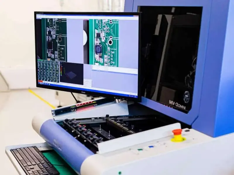
X-ray inspection is required for BGA and QFN packages where solder joints are hidden under the component. X-ray detects voids, opens, shorts, and misalignment that AOI cannot see.
If your design includes BGA or QFN packages, confirm that your assembler has X-ray inspection capability. Also confirm that the inspection criteria are defined before the build, not after.
Inspection du premier article
First-article inspection is the first physical check of the assembled board. It verifies that the placement, soldering, and connections match the design intent. The inspector checks the BOM against the placed components, verifies polarity and orientation, and confirms that the board functions as designed.
The first-article inspection is the last line of defense against symbol and footprint errors. If the inspector cannot verify a connection because the symbol used generic pin names, the board should be rejected until the discrepancy is resolved.
When to Escalate to Your Manufacturing Partner
Some issues cannot be resolved during design review. If you encounter any of the following, escalate to your manufacturing partner before proceeding:
- A component with an unusual package that does not match standard land patterns
- A board stackup that requires special stencil design or reflow profiling
- A BOM with components that have long lead times or are at risk of obsolescence
- A design that requires via-in-pad, edge plating, or other special processes
Your manufacturing partner can provide guidance on stencil design, paste release, reflow profiles, and inspection methods. They can also flag issues that you may not have considered, such as component clearance for pick-and-place nozzles or panelization constraints.
Omini, as an EMS provider, evaluates these factors during the DFM review and provides feedback before the build. This early involvement reduces the risk of assembly failures and costly rework.
Summary of Risk Evaluation Criteria
| Risk Factor | Que vérifier | Failure Mode |
|---|---|---|
| Symbol pin count | Compare against datasheet and footprint | Opens, shorts, misalignment |
| Pin names | Use standard names matching datasheet | Netlist ambiguity, inspection failure |
| Polarity markers | Verify pin 1 orientation | Backward placement, board failure |
| Thermal pad net | Confirm connection in symbol | Poor thermal performance, voids |
| BGA ball count | Count against datasheet | Misalignment, opens |
| BOM reference designators | Cross-check against schematic | Missing or duplicated components |
| Centroid file | Generate from layout, verify against BOM | Wrong placement, missed components |
| Coordinate system | Match between centroid and Gerber | Systematic placement offset |
Evaluate these factors before sending files to your PCBA partner. The time spent on design review is a fraction of the cost of a failed prototype run.
> Engineering handoff note: How to Evaluate SMT Assembly Risk from Packaging and Hybrid Bonding before the release package is frozen.
> Engineering handoff note: How to Evaluate SMT Assembly Risk from Consumer Electronics and Smartphone Trends before the release package is frozen.
> Engineering handoff note: How to Evaluate SMT Assembly Risk from PCB Design and Conformal Coating before the release package is frozen.