
Direct Answer
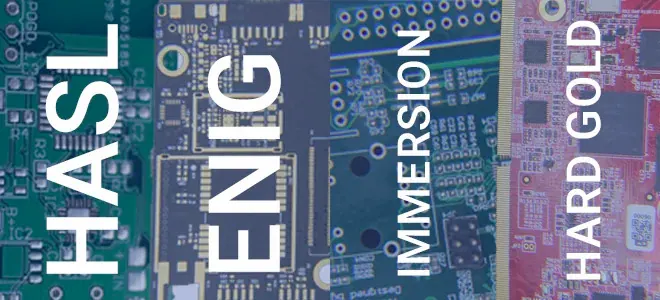
ENIG means electroless nickel immersion gold: a nickel barrier is deposited over exposed copper and immersion gold protects the nickel before soldering.
When To Use It
Use ENIG for BGA, QFN, fine-pitch SMT, longer bare-board storage, and assemblies where pad flatness is more important than the lowest surface-finish cost.
The first-principles check is whether ENIG PCB Surface Finish changes a real engineering decision. If the same files, inspection plan, stackup review, and acceptance criteria would be used without it, the entity probably belongs as a note on another page instead of a separate specification line.
Limits
ENIG depends on plating chemistry control, adds cost, and the nickel layer can be a disadvantage in some RF or contact applications.
This page avoids numeric limits unless the value can be tied to the exact standard, material grade, package note, or fabricator capability being used. Treat the reference as a decision boundary, not a substitute for the released fabrication drawing.
Manufacturing Or Assembly Impact
ENIG PCB Surface Finish must be visible in the RFQ when it changes CAM review, stackup selection, process flow, inspection depth, soldering risk, or test evidence. The buyer owns design intent and acceptance criteria; the manufacturer owns DFM feedback, process feasibility, and build evidence.
Comparison
Use ENIG for BGA, QFN, fine-pitch SMT, longer bare-board storage, and assemblies where pad flatness is more important than the lowest surface-finish cost.
The comparison should stay practical: choose the simpler option when it meets the electrical, thermal, assembly, and inspection requirements; choose the more controlled option only when it removes a real build risk.
Example
A dense BGA control board that may wait before assembly is a practical ENIG candidate when the drawing names the finish requirement and inspection expectations.
A useful quote package names the design files, revision, quantity, lead time, stackup or assembly constraints, inspection scope, and any source-controlled requirement. Missing assumptions should be closed before fabrication or assembly starts, because late discovery usually changes cost, schedule, or yield.
Source Notes
- ENIG finish specification boundary - IPC-4552 ENIG plating standard (standard).
Source fact: IPC-4552 is the source boundary for electroless nickel immersion gold surface-finish specification context. Omini interpretation: Use this to frame ENIG as a controlled fabrication finish that must be named in drawings and verified by the fabricator. Allowed usage: Use on ENIG entity, finish comparison, and surface-finish decision pages.
- IPC standards source boundary - IPC official resources (standard).
Source fact: IPC official resources are used to locate standards context and public summaries, while paid standard text remains outside the repository. Omini interpretation: Use this to separate standards-backed engineering framing from copied acceptance criteria or unsupported numeric claims. Allowed usage: Use when a page needs IPC context but does not have a narrower public source registered yet.
- Existing OminiPCB repository content (internal): May seed structure and internal links; engineering claims still need external verification when specifications are involved.
Practical notes on this page are manufacturing review guidance. They should not be read as copied standard text, datasheet tables, certification claims, or legal advice.
CTA
Request a PCB quote when Gerber, stackup, BOM, quantity, lead time, and inspection requirements are ready for engineering review.