
Direct Answer
IPC-A-600 Class 2 vs. Class 3: What are the Main Differences should be answered through engineering constraints, supplier capability, and RFQ evidence before release. The decision hinges on your product's end-use environment and the consequences of field failure, not on a desire to "be better.". If your board will face high vibration, thermal cycling, humidity, or if failure could cause injury or mission loss, Class 3 is the appropriate selection.
What IPC-A-600 Class 2 and Class 3 Actually Define
IPC-A-600 is the industry-accepted standard that defines the acceptance criteria for bare PCBs—the board before any components are placed. It covers the physical and electrical characteristics of the fabricated board, including copper plating, internal voids, dielectric spacing, annular ring tolerances, and surface conditions. The standard is organized into three classes: Class 1 (general electronics), Class 2 (dedicated service electronics), and Class 3 (high-reliability electronics). For most design and manufacturing decisions, the comparison comes down to Class 2 versus Class 3.
The practical difference is not about "good" versus "bad" boards. Both classes produce functional PCBs. The difference lies in the strictness of the acceptance criteria for internal and external defects. Class 2 allows minor imperfections—such as small edge chips, slight copper plating variations, or minor dielectric voids—provided they do not affect the board's function or reliability in a typical commercial environment. Class 3 imposes tighter limits on these same features because the board must survive harsher conditions and longer service life without failure.
For example, consider a copper void in an internal layer. Under Class 2, a small void that does not reduce the conductor's cross-sectional area below a functional threshold may be acceptable. Under Class 3, the same void might be rejected because it could act as a stress concentration point under thermal cycling or vibration. The inspection criteria are defined in IPC-A-600, but the manufacturing process—the lamination, drilling, plating, and etching—remains essentially the same. The difference is in how much defect you are willing to accept and how much inspection you are willing to pay for.
Direct Answer: Which Class Should You Choose for Production?
For most commercial and industrial products, Class 2 is the safer production choice because it allows minor cosmetic and edge defects that do not affect function, while Class 3 is safer for life-critical or high-reliability systems where even a small void or crack can lead to field failure.
The conditions that change this answer are straightforward. If your product operates in a benign environment—indoor, controlled temperature, minimal vibration—Class 2 will meet your needs and keep costs down. If your product will be implanted in a medical device, deployed in an aerospace avionics bay, or mounted on a vehicle suspension system, Class 3 is not optional; it is a requirement. Similarly, if your customer contract or industry standard (e.g., medical, aerospace, defense) explicitly mandates Class 3, the decision is made for you. The key is to base the choice on engineering data and end-use requirements, not on a general assumption that "higher class equals better."
Another condition that changes the decision is the component package type. If your board uses BGAs, fine-pitch QFPs, or other packages where solder joint integrity is critical and internal inspection is required, Class 3 inspection criteria may force you to use X-ray and microsection analysis. This increases cost and lead time. If your design uses only through-hole or larger-pitch components, Class 2 may be perfectly adequate even in moderately demanding environments.
Reliability: How Class 3 Differs in Internal and External Criteria
Reliability is the primary driver for choosing Class 3. The standard requires stricter control of internal voids, copper plating thickness, and dielectric integrity. For example, IPC-A-600 Class 3 typically requires a higher minimum copper plating thickness in the barrel of plated through-holes compared to Class 2. This is because the barrel of a via or through-hole is a common failure point under thermal cycling; a thinner plating can crack, breaking the electrical connection.
Similarly, internal dielectric spacing requirements are tighter for Class 3. In a Class 2 board, a slight reduction in dielectric thickness between layers might be acceptable if it does not cause a short. In a Class 3 board, the same reduction could be rejected because it increases the risk of dielectric breakdown under high voltage or high humidity. The acceptance criteria are defined in IPC-A-600, but the practical effect is that the fabricator must use tighter process controls—better lamination pressure, more consistent etch rates, and more rigorous cleaning—to meet Class 3.
From a manufacturing consequence perspective, Class 3 does not change the base materials or the fabrication steps. You still use the same FR-4, polyimide, or high-speed laminate; you still drill, plate, and etch. What changes is the tolerance you must hold and the amount of inspection required to verify those tolerances. This is why Class 3 boards cost more: the fabricator must spend more time on process control and verification, and they must scrap boards that would have passed Class 2 but fail Class 3.
Assembly Yield: How Class Choice Affects Solder Joint Reliability
The class choice also affects assembly yield, particularly for solder joints. Class 3 requires stricter control of solder joint fillet size, wetting, and voiding. For example, in a Class 2 board, a small void in a BGA solder ball might be acceptable if it does not reduce the joint's electrical or mechanical integrity. In a Class 3 board, the same void might be rejected because it could propagate under thermal stress.
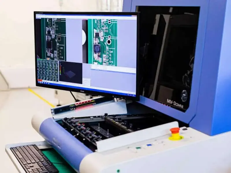
This is where the inspection method becomes critical. Visual inspection is not sufficient for Class 3 BGA joints. You need X-ray inspection to see the internal voids and solder ball shape. Similarly, microsection analysis—cutting the board and polishing a cross-section—is often required to verify copper plating thickness and internal layer registration. These are destructive tests, so they are performed on a sample basis, but they add to the inspection cost and lead time.
For assembly, the practical consequence is that Class 3 boards often require a more controlled reflow profile. If your reflow profile has a wide temperature delta across the board, you may create more voids in the solder paste, which is acceptable under Class 2 but not under Class 3. This means your SMT assembly process must be tuned more carefully, and you may need to use a slower ramp rate or a longer soak zone to minimize voiding.
If you are working with a contract manufacturer, they will need to know the class requirement upfront so they can adjust their process accordingly. For more on how reflow profiles affect solder joint quality, see Differences Between Reflow Soldering and Wave Soldering.
Cost Drivers: Where Class 3 Adds Expense
The cost difference between Class 2 and Class 3 is not fixed; it depends on board complexity, layer count, and the specific acceptance criteria you choose. However, there are several consistent cost drivers. First, inspection costs are higher for Class 3. You will likely need 100% AOI on the bare board, X-ray for BGAs and other hidden joints, and microsection analysis for internal verification. Each of these adds time and requires specialized equipment.
Second, the tighter tolerances mean more scrap. If a fabricator runs a panel with eight boards and one board has a minor copper void that passes Class 2 but fails Class 3, they must scrap the entire panel or at least rework the defective board. This drives up the per-board cost. Third, the documentation burden is higher for Class 3. You may need to provide a detailed stackup, material certifications, and test reports. This adds administrative overhead.
Finally, the fabrication process itself may need to be adjusted. For example, to meet Class 3 copper plating requirements, the fabricator may need to use a slower plating process or a more expensive electrolytic copper bath. This increases the cost per board. The same applies to drilling: Class 3 may require smaller drill bits or more precise registration, which increases tooling wear and cost.
> Practical note: If you are on a tight budget and your product operates in a benign environment, do not default to Class 3 just to "be safe." The cost increase can be 20–40% or more, and you will not see a reliability benefit if the board never experiences harsh conditions. Instead, focus on the specific failure modes that matter for your application.
Inspection Limits: What AOI, X-ray, and Microsection Can and Cannot See
Inspection is where Class 2 and Class 3 diverge most in practice. Class 2 relies heavily on visual inspection and standard AOI. AOI is excellent for detecting missing components, wrong polarity, and gross solder defects, but it cannot see inside a BGA joint or verify the internal structure of a via. For Class 3, you need X-ray for BGA and fine-pitch components, and microsection for internal verification.
X-ray inspection is essential for Class 3 because it reveals voids in solder joints, the shape of the solder ball, and the integrity of the via barrel. However, X-ray has limits. It cannot measure copper plating thickness directly; for that, you need microsection. Microsection is destructive, so it is performed on a sample basis—typically one or two boards per lot. This means you are verifying the process, not every board.
For a deeper look at how AOI coverage affects defect detection, see How to Choose SMT AOI Inspection Coverage for PCB Assembly Defects. The key takeaway is that Class 3 does not just require more inspection; it requires different types of inspection that see different layers of the board. If your contract manufacturer does not have X-ray or microsection capability in-house, they will need to outsource it, which adds lead time and cost.
Process Risk: How Class Choice Affects Fabrication and Assembly
Process risk is higher for Class 3 because the tighter tolerances leave less room for error. In fabrication, this means the laminate must be of consistent quality, the lamination pressure must be uniform, and the etching process must be tightly controlled. A slight variation in any of these can cause a defect that fails Class 3 but passes Class 2.
In assembly, the risk shifts to solder joint formation. Class 3 requires better wetting and fewer voids, which means the reflow profile must be optimized for the specific solder paste and component types. If you are using a lead-free solder like SAC305, the peak temperature and time above liquidus must be controlled carefully. Too much heat can cause pad lifting or intermetallic growth; too little heat can cause poor wetting. For a Class 2 board, a minor solder ball or a small void is acceptable. For Class 3, it is not.
The assembly process steps themselves are the same regardless of class. You still apply solder paste, place components, and reflow. The difference is in the process window. Class 3 requires a narrower process window, which means your equipment must be well-calibrated and your operators must be well-trained. If you are working with a new EMS provider, you should verify their process capability before committing to a Class 3 build. For an overview of the assembly steps, see Explained: What are the Steps in SMT Assembly Process?.
Common Mistakes and False Assumptions
One of the most common mistakes is assuming that Class 3 is always safer. This is false. Class 3 imposes stricter acceptance criteria, but it does not change the manufacturing process itself. If your fabricator uses the same process for Class 2 and Class 3, you are not getting a better board; you are just getting a board that has been inspected more strictly. The board is not inherently more reliable; it is just less likely to contain a defect that would fail the Class 3 criteria.
Another mistake is ignoring the need for X-ray on BGAs. Many designers assume that if the board passes electrical test, the solder joints are good. This is not true. Electrical test verifies continuity, but it cannot detect a cracked solder ball or a void that will fail after thermal cycling. If your design uses BGAs and you are building to Class 3, X-ray is not optional.
A third mistake is not sending enough stackup and BOM data for review. The fabricator needs to know the layer count, copper weight, and laminate material to assess whether Class 3 is achievable. They also need the BOM to understand the component package types and whether X-ray or microsection will be required. Without this data, they cannot give you an accurate quote or a realistic assessment of the risk.
Finally, do not assume that visual inspection is enough for Class 3. It is not. Class 3 requires microsection and X-ray for internal verification. If your contract manufacturer tells you they can do Class 3 with visual inspection alone, they are either misinformed or cutting corners.
Decision Matrix: Class 2 vs. Class 3
The table below summarizes the key differences and helps you make a quick decision based on your product's requirements.
| Criterion | Class 2 (Dedicated Service) | Class 3 (High-Reliability) |
|---|---|---|
| End-use environment | Commercial, industrial, benign | Harsh, life-critical, mission-critical |
| Failure consequence | Downtime, repair cost | Injury, mission loss, significant financial loss |
| Internal voids | Minor voids acceptable | Tighter limits; voids may be rejected |
| Copper plating | Standard thickness | Higher minimum thickness in PTH barrels |
| Inspection method | Visual, AOI, basic electrical test | AOI + X-ray + microsection (sample) |
| Process window | Wider; minor variations acceptable | Narrower; process must be tightly controlled |
| Cost impact | Baseline | 20–40% higher (typical) |
| Lead time | Standard | Longer due to additional testing |
| Documentation | Standard fabrication report | Detailed stackup, material certs, test reports |
What Data to Send for a Class 2 vs. Class 3 Review
To get an accurate review from a manufacturer like Omini, you need to send a complete fabrication and assembly package. This includes the Gerber files, stackup details (layer count, copper weight, laminate material), and the BOM with part numbers and package types. You should also include any notes on critical signals or impedance requirements. If you have specific acceptance criteria in mind—for example, IPC-A-600 Class 3 for internal voids—state that explicitly.
The operating environment is also important. If the board will be exposed to high vibration, thermal cycling, or humidity, say so. This information helps the manufacturer assess whether Class 3 is necessary or whether Class 2 would be sufficient. Finally, specify the expected inspection method. If you know you will need X-ray for BGAs, mention it. This allows the manufacturer to confirm they have the capability and to include the cost in the quote.
For a related comparison that focuses on the finished board (after assembly), see IPC 6012 Class 2 vs Class 3: What Are the Main Differences. While IPC-A-600 covers the bare board, IPC-6012 covers the qualification and performance of the finished board, and the class distinctions follow a similar logic.
FAQ
Which class is safer for production: Class 2 or Class 3?
For most commercial and industrial products, Class 2 is the safer production choice because it allows minor cosmetic and edge defects that do not affect function. Class 3 is safer for life-critical or high-reliability systems where even a small void or crack can lead to field failure. Your decision should be based on the end-use environment, not on a desire to "be better."
What factors should change my decision from Class 2 to Class 3?
The decision changes when the product must operate in harsh environments (vibration, thermal cycling, high humidity), when failure could cause injury or mission loss, or when the customer contract or industry standard (e.g., medical, aerospace, defense) mandates Class 3. Also, if your board uses BGAs or fine-pitch components, Class 3 inspection criteria may force you to use X-ray and microsection, which increases cost and lead time.
What data should I send to Omini for a Class 2 vs Class 3 review?
Send the complete fabrication and assembly package: Gerber files, stackup details (layer count, copper weight, laminate material), BOM with part numbers and package types, and any notes on critical signals or impedance requirements. Also specify the intended operating environment and the acceptance criteria you expect (e.g., IPC-A-600 Class 3 for internal voids). The more context you provide, the more accurate the review will be.
What are common false assumptions about Class 2 and Class 3?
A common false assumption is that Class 3 automatically means better quality. In reality, Class 3 imposes stricter acceptance criteria, but it does not change the manufacturing process itself. Another mistake is assuming that Class 2 boards are "good enough" for all applications; if your product will face high vibration or thermal stress, Class 3 may be required. Also, don't assume that visual inspection is enough—Class 3 often requires microsection and X-ray for internal verification.
How does Class 3 affect cost and lead time compared to Class 2?
Class 3 typically increases cost because it requires more stringent inspection (e.g., 100% AOI, X-ray for BGAs, microsection), tighter tolerances, and more documentation. It can also lengthen lead time due to additional testing and corrective action steps. However, the cost difference is not fixed—it depends on board complexity, layer count, and the specific acceptance criteria you choose.
Should I use flying probe or ICT for Class 3 boards?
Flying probe testing is a good option for Class 3 boards, especially in low-to-medium volume production, because it does not require a custom test fixture and can be programmed quickly. However, flying probe is slower than ICT. For high-volume Class 3 production, ICT with a custom fixture may be more cost-effective. The choice depends on your volume, budget, and the test coverage you need. For more details, see Demystifying Flying Probe PCB Testing: The What, Why, and How.
> Engineering handoff note: IPC-600 Classes: Differentiating Between Class 1, 2, and 3 PCBs before the release package is frozen.