
Direct Answer
For most commercial and industrial electronics, IPC 6012 Class 2 is the recommended choice because it balances reliability with manufacturability and cost. Choose Class 3 only when failure causes safety risks, mission-critical downtime, or expensive field repairs. The decision changes based on operating environment, failure consequences, and required service life, not on a general preference for higher certification.
The Engineering Difference Between Class 2 and Class 3
IPC 6012 defines the qualification and performance requirements for rigid printed boards. The standard establishes three performance classes, with Class 2 covering dedicated service electronic products and Class 3 covering high-reliability electronic products where continued performance is critical. The difference is not a simple quality rating; it is a set of measurable fabrication criteria that affect how a board is built, inspected, and accepted.
Class 2 permits limited cosmetic imperfections and minor defects as long as the board functions reliably in its intended application. Class 3 demands tighter tolerances on copper thickness, stricter hole wall quality, and more conservative defect acceptance limits. The manufacturing consequence is that Class 3 boards require more precise process control, additional inspection steps, and often lower panel utilization because of tighter spacing rules.
Copper Thickness and Plating Tolerance
The most visible engineering difference appears in copper thickness requirements. Class 2 allows a wider tolerance band on finished copper thickness, both on surface conductors and in plated through-holes. Class 3 requires tighter control over the minimum copper thickness in the barrel of the hole, especially after drilling and plating processes.
For a standard 1 oz (35 µm) outer layer, Class 2 might accept a finished thickness that dips slightly below nominal in isolated areas. Class 3 requires the minimum to hold across the entire board surface and within every plated hole. This affects your stackup design because the target copper weight must be specified with the class in mind. If you design a 0.5 oz base copper with 1 oz plating for a Class 3 board, the manufacturer must verify that the final plated thickness meets the minimum everywhere, not just in the coupon test areas.
Hole Wall Quality and Microsection Requirements
Hole wall quality is where Class 3 requirements become significantly more demanding. Class 3 boards require microsection analysis to verify that the plated copper in the hole wall is continuous, void-free, and properly bonded to the inner layers. The acceptable void size, the amount of etch-back, and the condition of the resin smear are all evaluated more strictly.
For Class 2, a small void in the hole wall might be acceptable if it does not reduce the effective cross-section below the minimum. For Class 3, the same void could be cause for rejection. This is not a theoretical concern: a void in a high-current via can create a hot spot that eventually cracks under thermal cycling. If your design uses high-layer-count boards with thick dielectric materials, the drilling and desmear process must be tuned to meet Class 3 hole wall criteria.
Reliability, Assembly Yield, and Cost Drivers
The choice between Class 2 and Class 3 affects more than the bare board fabrication. It influences assembly yield, inspection strategy, and total cost across the product lifecycle.
Reliability in the Field
Class 3 boards are designed for applications where downtime is unacceptable. The tighter copper tolerances and stricter hole wall criteria directly address the most common field failure modes: via cracking, barrel fatigue, and conductor separation under thermal stress. If your product operates in a high-vibration environment, experiences frequent thermal cycling, or carries high current density, Class 3 provides a measurable reliability margin.
Class 2 boards are reliable in benign environments. A consumer device that operates indoors at moderate temperatures, with low vibration and minimal thermal cycling, will typically perform well with Class 2 fabrication. The reliability difference only becomes visible when the operating conditions push the board toward its limits.
Assembly Yield and Rework
Class 3 boards are more expensive to assemble because the tighter tolerances reduce the margin for error during soldering. For example, a Class 3 board with tighter annular ring requirements leaves less room for component placement misalignment. If your pick-and-place machine has a placement accuracy of ±50 µm, a Class 3 board with a 75 µm annular ring requirement will produce more placement-related defects than a Class 2 board with a 100 µm requirement.
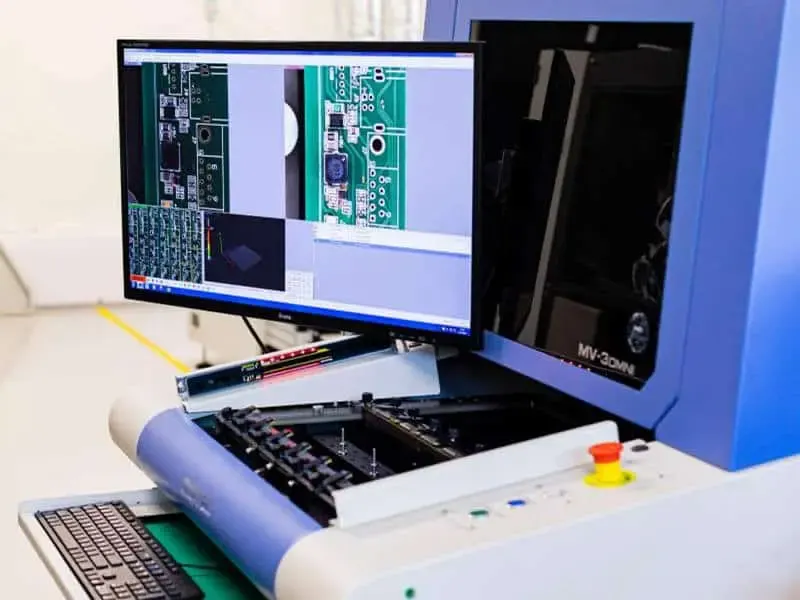
The inspection burden also increases. Class 3 boards typically require more extensive AOI coverage during SMT assembly and may require X-ray inspection for BGAs and other hidden joints. This adds time to the assembly process and increases the cost per board. The rework risk is also higher because the tighter tolerances make manual rework more difficult without violating the acceptance criteria.
Cost Drivers
The cost difference between Class 2 and Class 3 comes from several sources:
- Panel utilization: Class 3 spacing rules often force lower panel density, increasing the board area cost.
- Inspection time: Class 3 requires more microsections, more AOI passes, and more detailed documentation.
- Process control: Tighter copper and hole wall tolerances require more frequent monitoring of the plating line and drilling parameters.
- Yield loss: The stricter acceptance criteria mean that boards that would pass Class 2 inspection may be rejected under Class 3, raising the effective cost of good boards.
- Testing: Class 3 boards may require more extensive electrical testing, including flying probe testing for all nets rather than a sample.
For a typical 4-layer board, the cost increase from Class 2 to Class 3 is modest. For a 12-layer board with impedance control and via fill, the cost increase can be substantial because the yield loss and inspection burden multiply with layer count.
Comparison Matrix: Class 2 vs Class 3
| Criterion | IPC 6012 Class 2 | IPC 6012 Class 3 |
|---|---|---|
| Primary use case | Commercial, industrial, consumer electronics | Medical, aerospace, military, mission-critical systems |
| Copper thickness tolerance | Wider tolerance band | Tight tolerance, minimum verified across board and holes |
| Hole wall quality | Minor voids acceptable if function is preserved | Voids strictly limited; microsection verification required |
| Annular ring requirement | Standard tolerance | Tighter tolerance for higher reliability |
| Inspection rigor | AOI, sample microsection, electrical test per plan | More extensive AOI, X-ray, microsection, full traceability |
| Assembly margin | More forgiving of placement variation | Less margin; placement accuracy matters more |
| Field failure tolerance | Acceptable for replaceable or benign-environment products | Designed for continuous operation without failure |
| Relative cost | Lower fabrication and inspection cost | Higher fabrication, inspection, and assembly cost |
| Common failure mode if misapplied | Premature via failure in harsh environments | Over-specified cost for products that do not need it |
Process Risk and Inspection Limits
The inspection methods available to your manufacturer set a practical limit on what class you can realistically target. Class 3 requires verification of internal features that cannot be seen from the outside. This means microsection analysis, which destroys a coupon or a test board, and X-ray inspection for internal alignment.
Microsection Analysis
Microsectioning is the primary method for verifying hole wall quality, copper thickness, and layer-to-layer registration. For Class 3, the manufacturer must perform microsection analysis on a defined frequency, typically per lot or per panel. The results must be documented and traceable to the specific production lot.
If your manufacturer does not have a reliable microsection process, or if their sampling plan is not rigorous enough, a Class 3 claim is not trustworthy. Ask your manufacturer how they sample microsections, how many coupons per panel they analyze, and what their acceptance criteria are for void size and copper thickness.
Electrical Testing
Class 3 boards require 100% electrical testing for continuity and isolation. This is typically done with a flying probe tester or a bed-of-nails fixture. The test program must cover all nets, and the test data must be traceable to the specific board serial number.
For Class 2, the testing requirement is also 100% in most cases, but the acceptance criteria for resistance values and isolation thresholds may be more lenient. If your design has high-density BGA packages with fine pitch, the test fixture design becomes critical. A poorly designed test fixture can miss a short between adjacent vias, which would be a field failure.
The Role of AOI and X-Ray in Assembly
During assembly, the inspection strategy must match the board class. Class 3 boards benefit from automated optical inspection (AOI) with high coverage on both the solder paste and the placed components. X-ray inspection is recommended for BGAs, QFNs, and other packages where the joints are hidden.
The practical consequence is that a Class 3 board with a complex BGA design will require X-ray inspection of every board, not a sample. This adds cycle time and cost. If your product is a high-volume consumer device, the added inspection cost per board may not be justified.
Common Mistakes and False Assumptions
Mistake 1: Assuming Class 3 Is Always Better
Class 3 does not guarantee better electrical performance, better solderability, or better assembly quality. It guarantees tighter fabrication tolerances and stricter acceptance criteria. A Class 3 board with poor solder paste printing will fail just as fast as a Class 2 board. The class does not compensate for poor assembly process control.
Mistake 2: Using Class 2 for Mission-Critical Systems
If your product is a medical device, an avionics module, or a server that must never go down, Class 2 may not provide the reliability margin you need. The failure mode is often via barrel cracking after thousands of thermal cycles. Class 3's tighter copper thickness and hole wall requirements directly reduce the probability of this failure.
Mistake 3: Ignoring the Impact on Panel Utilization
Class 3 spacing rules can reduce the number of boards per panel. This is a real cost driver that is often overlooked during design. If you are designing a high-volume product, the panel utilization difference between Class 2 and Class 3 can be significant.
Mistake 4: Not Sending the Right Data for Review
To get an accurate quote and a manufacturable design, send the complete fabrication package: Gerber files, drill files, stackup details with copper weights and dielectric materials, impedance requirements, and a clear statement of the target IPC class. If you have special requirements like via fill, controlled impedance, or a specific surface finish, include those as well. The manufacturer needs this data to verify that the design meets the class before quoting.
> Practical note: When you specify Class 3, ask your manufacturer to confirm that their standard process can meet the requirements without special engineering. Some manufacturers quote Class 3 but actually build to a relaxed internal standard. Request a copy of their Class 3 capability matrix and their microsection sampling plan before you commit.
When the Choice Changes: Decision Factors
The decision between Class 2 and Class 3 is not static. It changes based on the product's end-use environment, the cost of failure, and the required service life.
Operating Environment
If the board operates in a controlled indoor environment with stable temperature and low vibration, Class 2 is usually sufficient. If the board operates outdoors, in a vehicle, or near a heat source, the thermal cycling and vibration will stress the vias and conductors. Class 3 provides a measurable margin in these conditions.
Cost of Failure
Consider what happens when the board fails. If the failure means a field replacement under warranty, a recall, or a safety incident, Class 3 is justified. If the failure means the user replaces a $50 device, Class 2 is the right economic choice.
Service Life
Class 3 boards are designed for long service life under continuous operation. If your product is expected to operate for 10 years without maintenance, Class 3 provides the reliability margin. If the product is replaced every 2-3 years, Class 2 is sufficient.
Material Selection
The choice of laminate material interacts with the IPC class. For high-frequency designs, the RF PCB material selection affects the achievable tolerances. A high-speed digital design with tight impedance control may require a material with a stable dielectric constant, which can be more expensive and harder to process. The IPC class does not change the material selection, but it does change the acceptable tolerance on the final impedance value.
For heavy copper and power PCB designs, the copper thickness tolerance becomes even more critical. A Class 3 heavy copper board requires very tight control over the plated copper thickness, which is harder to achieve with 4 oz or 6 oz copper. The plating process must be carefully controlled to avoid over-plating the holes while still meeting the surface copper requirement.
Assembly Process
The soldering process choice also interacts with the IPC class. A Class 3 board with a mixed-technology design (SMT and through-hole) may require both reflow and wave soldering. The thermal profile of the wave soldering process can stress the plated holes, and the tighter Class 3 hole wall requirements make the process window smaller.
What to Send for a Class 2 or Class 3 Review
To get an accurate quote and a manufacturable design, send the following to your PCB manufacturer:
1. Gerber files and drill files in the standard format (RS-274X or ODB++). 2. Stackup details including copper weights, dielectric materials, and layer count. 3. Impedance requirements if your design has controlled impedance traces. 4. A clear statement of the target IPC class (Class 2 or Class 3). 5. Special requirements such as via fill, surface finish, or specific solder mask color. 6. Assembly notes if you are also contracting assembly, including BOM status and any special handling requirements.
The manufacturer will use this data to verify that the design meets the class requirements before quoting. If the design has features that conflict with the class, such as annular rings that are too small for Class 3, the manufacturer should flag this during the DFM review.
Omini acts as a manufacturing partner that reviews your design against the target class, identifies potential issues, and provides a realistic quote based on your actual requirements. Sending the complete package ensures that the quote reflects the real cost of building to the specified class.
FAQ
Which IPC 6012 class is safer for production?
For most commercial and industrial products, Class 2 is safer because it balances reliability with cost and manufacturability. Class 3 is safer only when your product must operate continuously without failure, such as in medical, aerospace, or military systems. Choose based on the consequence of failure, not on a general preference for a higher class.
What changes the decision between Class 2 and Class 3?
The main factors are the product's operating environment, the cost of failure, and the required service life. If a PCB failure causes downtime, safety risks, or expensive repairs, Class 3 is justified. For consumer devices or equipment where a failure is easily replaced, Class 2 is usually sufficient. Also consider inspection capabilities and your budget.
What data should I send for a Class 2 or Class 3 review?
Send the complete fabrication package: Gerber files, drill files, stackup details with copper weights and dielectric materials, impedance requirements, and a clear statement of the target IPC class. Also include any special requirements like controlled impedance, via fill, or a specific surface finish. This allows the manufacturer to verify that the design meets the class before quoting.
What are common false assumptions about IPC 6012 classes?
A common false assumption is that Class 3 PCBs are always higher quality in every aspect. In reality, Class 3 focuses on specific fabrication criteria like copper thickness, hole wall quality, and defect limits, but it does not guarantee better electrical performance or assembly quality. Another false assumption is that Class 2 is always unreliable; many Class 2 boards last for years in benign environments.
> Engineering handoff note: Demystifying Flying Probe PCB Testing: The What, Why, and How, Differences Between Reflow Soldering and Wave Soldering, and Heavy Copper & Power PCBs: Exploring the World before the release package is frozen.
> Also compare How to Choose SMT AOI Inspection Coverage for PCB Assembly Defects and How Do You Select RF PCB Material and the Most Commonly Used Types? before locking the quote scope.