
Direct Answer
RoHS regulations fundamentally reshape PCB production by restricting hazardous substances, with lead being highly relevant for solder and surface finishes. Compliance requires lead-free assembly, which demands higher reflow temperatures, revised material selections, and updated testing protocols to maintain performance and reliability. For Omini RFQs, RoHS expectations should be stated early so material, finish, assembly, documentation, and test assumptions are visible before release.
Material Selection Under RoHS
RoHS directly governs the raw materials used in PCB fabrication, starting with the laminate. While FR-4 itself is not restricted, the resin systems and flame retardants must comply with limits on substances like polybrominated biphenyls (PBB) and polybrominated diphenyl ethers (PBDE). Manufacturers now use halogen-free or phosphorus-nitrogen-based flame retardants to meet these thresholds, which can affect glass transition temperature (Tg) and moisture absorption. These changes necessitate updated storage and pre-bake procedures to prevent delamination during assembly.
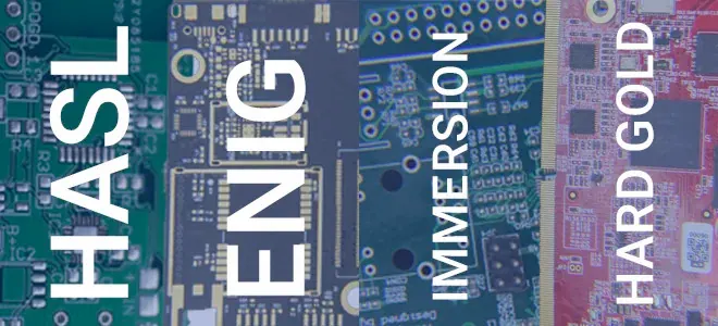
Copper foil remains largely unaffected, but surface finishes are heavily impacted. Lead-based Hot Air Solder Leveling (HASL-Lead) is prohibited, pushing the industry toward alternatives like Electroless Nickel Immersion Gold (ENIG), Organic Solderability Preservative (OSP), immersion tin, and immersion silver. ENIG dominates high-reliability applications due to its flat surface, excellent solderability with lead-free alloys, and resistance to oxidation. OSP is cost-effective for consumer electronics but requires strict control of handling and storage time, as it degrades quickly when exposed to humidity or contaminants. Immersion tin offers good solderability but risks whisker formation and tin pest in cold environments, while immersion silver provides good conductivity but is prone to tarnishing and sulfide corrosion.
These finish choices are not interchangeable. For example, ENIG is often preferred for fine-pitch BGAs and QFNs due to its planar surface, which can reduce solder bridging and voiding risk. OSP, while economical, can lead to poor wetting if boards are stored beyond their shelf life or exposed to oils from handling. The RFQ should define which compliance documents, finish evidence, and first-article checks are required.
Lead-Free Assembly and Process Adjustments
The shift to lead-free solder alloys—primarily SAC305 (Sn-Ag-Cu)—has the most profound impact on PCB assembly. These alloys melt at approximately 217–220°C, significantly higher than the 183°C eutectic point of SnPb solder. This necessitates reflow peak temperatures of 240–250°C, with tighter tolerances on time-above-liquidus (TAL) to avoid overheating components or under-reflowing joints.
Higher temperatures affect every aspect of the assembly process. Component selection must prioritize parts rated for lead-free reflow, as some older or cost-sensitive devices may suffer internal damage, delamination, or popcorning at elevated thermal loads. Thermal management in the stackup becomes critical: thicker copper layers or thermal vias may be needed to dissipate heat evenly during reflow, especially in high-power designs. Conversely, excessive copper can act as a heat sink, making it harder to reach peak temperature—requiring adjustments to the reflow profile’s ramp rate and soak time.
Solder paste performance is another key consideration. Lead-free pastes have different wetting characteristics, flux activity, and slump behavior. They are more prone to oxidation and require controlled storage and handling. Voiding in BGAs and QFNs is a common defect linked to outgassing from fluxes or moisture trapped under the component, exacerbated by longer TAL in lead-free processes. The assembly plan should define the inspection method and acceptance criteria for voiding when hidden solder joints are a risk.
DFM checks should verify lead-free process windows. This includes validating solder paste stencil design for adequate release, checking pad sizes for sufficient solder volume, and ensuring clearance around thermal vias to prevent solder wicking away from joints. For designs with heavy copper, the interaction between thermal mass and lead-free reflow becomes even more pronounced because thicker copper layers can create localized cold spots. Thermal balancing techniques, such as copper thieving or staggered via placement, may be reviewed during DFM.
Surface Finish Compatibility and Reliability
The choice of surface finish is not just about compliance; it directly influences solder joint reliability under lead-free conditions. ENIG's nickel layer acts as a barrier to copper diffusion, but excessive nickel thickness can contribute to brittle intermetallic behavior and fracture risk under thermal cycling. Finish thickness requirements and evidence should be defined in the fabrication drawing or quality plan.
OSP finishes rely on a thin organic layer that volatilizes during reflow, exposing clean copper for solder bonding. However, if the OSP layer degrades prematurely due to humidity or contamination, it can leave behind residues that inhibit wetting, leading to non-wet opens or weak joints. This is particularly problematic in high-mix environments where boards may sit in queue for extended periods. Handling and floor-life assumptions should be defined before release.
Immersion tin and silver finishes present their own challenges. Tin can form intermetallics with silver in the solder alloy, while silver is susceptible to sulfur-induced tarnishing, which increases contact resistance and reduces solderability. Both require careful packaging and shelf-life controls. For high-reliability applications such as automotive or industrial controls, finish selection should be justified by assembly method, operating environment, shelf life, and customer acceptance criteria.
Testing protocols have evolved to validate these interactions. Beyond standard electrical testing, cross-sectioning, thermal cycling, humidity bias testing, or lab analysis may be required for harsh field conditions. The RFQ should state which tests and records are required rather than treating them as default compliance evidence.
Testing, Documentation, and Supply Chain Control
Verifying RoHS compliance requires more than a single test; it demands material traceability, supplier validation, and ongoing monitoring. A buyer file may require declarations of conformity (DoC) for laminates, prepregs, copper foil, surface finishes, solder pastes, fluxes, and cleaning agents. When lab evidence is required, the accepted test method should be specified by the customer or compliance owner.
XRF screening is a common non-destructive first pass for restricted-substance review. If XRF indicates a potential exceedance, samples may need lab confirmation using wet chemical methods. The required evidence level should match the market, product risk, and buyer compliance file.
Batch traceability should connect panels or assemblies to material lot numbers, supplier declarations, and production records when the buyer requires that evidence. This is especially critical when dealing with exemptions; any exemption build should have a documented segregation and approval plan owned by the product and compliance stakeholders.
Final validation may include functional testing and compliance documentation packages when requested. Material declarations, test reports, and assembly records support the customer's due-diligence file under applicable regulations. These documents are essential for market access in regions that inspect electronic goods for restricted substances.
Cost, Yield, and Long-Term Viability
While the initial transition to lead-free manufacturing increased costs due to higher energy consumption, material changes, and lower yields, RoHS-compliant processes are now mature in many PCB and PCBA environments. The industry has optimized solder pastes, reflow ovens, and flux formulations specifically for lead-free assembly, narrowing the performance gap with SnPb processes.
Panelization and design for manufacturability (DFM) play a larger role in maintaining efficiency. For example, balancing copper distribution across the panel prevents warpage during high-temperature reflow, which can cause misalignment and solder defects. Similarly, optimizing solder paste stencil design—using step stencils or local thickness variations—helps accommodate mixed-technology boards where heavy copper areas require more solder while fine-pitch components need less. These adjustments are informed by real-world data from production runs, not theoretical models.
During design review, teams should anticipate RoHS-related challenges by reviewing Gerber files for finish compatibility, checking component datasheets for lead-free reflow ratings, and considering stackup adjustments to manage thermal mass. By integrating these checks early, similar to the DFM principles outlined in resources like Common DFM Issues and How to Avoid Them in PCB Design, the need for late-stage redesigns is reduced.
Ultimately, RoHS compliance is not a barrier to innovation but a catalyst for more robust, sustainable PCB production. The restrictions on hazardous substances have driven improvements in material science, process control, and testing rigor that benefit electronic products across markets. For Omini buyers, the key is to state RoHS expectations, evidence needs, and acceptance criteria before quote so the manufacturing plan reflects the actual compliance scope.
Related Omini Engineering Notes
- Common DFM Issues and How to Avoid Them in PCB Design
- Common Failures in Heavy Copper PCB and How to Avoid Them in the Design Stage
- Common PCB Defects and How to Identify Them
- Different Production Process Between Heavy Copper PCB and FR4 PCB
- Guide to Testing PCB Boards: Everything You Need to Know